

Semiconductor light emitting device package
a technology of light-emitting devices and semiconductors, which is applied in the direction of semiconductor devices, basic electric elements, electrical appliances, etc., can solve the problems of light loss and color purity degrade, and achieve excellent color purity, luminance, and efficiency.
- Summary
- Abstract
- Description
- Claims
- Application Information
AI Technical Summary
Benefits of technology
Problems solved by technology
Method used
Image

Examples
embodiment 1
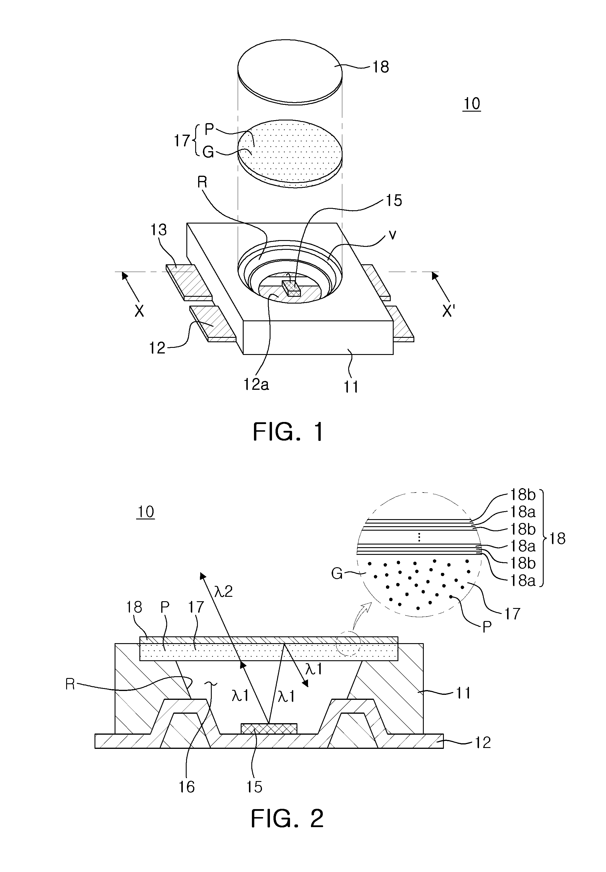
[0117]LED packages were manufactured to be similar to that of comparative example 1, and an optical filter was additionally applied to the wavelength conversion unit. Namely, an α-SiAlON phosphor and a ZnO—BaO—SiO2—P2O5—B2O3-based glass composition were mixed in a blue LED chip having a wavelength of 445 nm, shaped as a film, the film was sintered at a temperature of 420° C., and the sintered film was polished to form a wavelength conversion unit having a thickness equal to 100 μm.
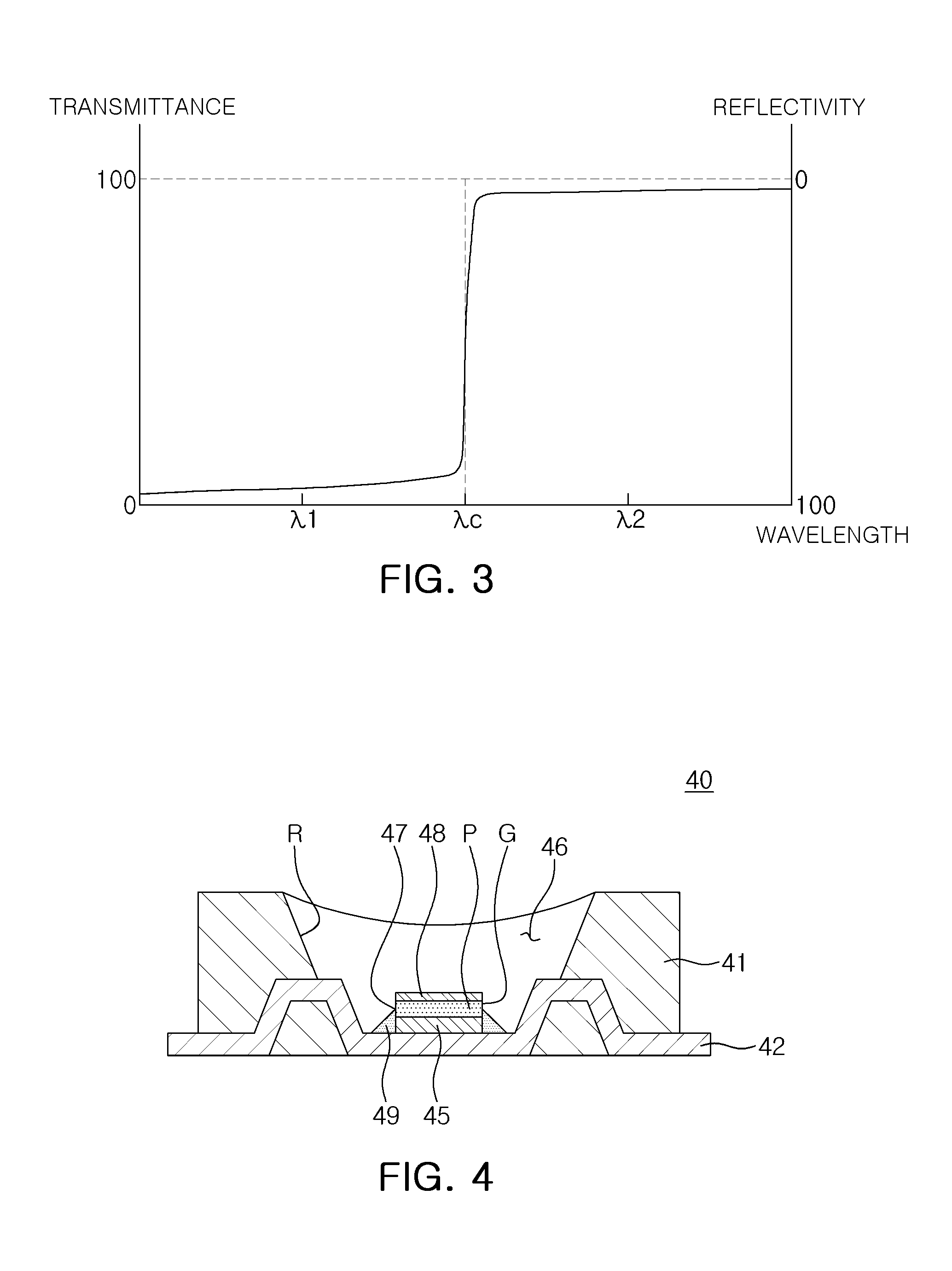
[0118]Eight wavelength conversion units were manufactured by changing a mixing ratio (weight ratio) between the α-SiAlON phosphor and the ZnO—BaO—SiO2—P2O5—B2O3-based glass composition to 1 / 200, 1 / 100, 1 / 60, 1 / 20, 1 / 15, 1 / 10, 1 / 6, 1 / 3, and a wavelength selective optical film cutting off a wavelength equal to or lower than 500 nm was formed. In detail, an SiO2 film having a thickness equal to 25 nm and a TiO2 film having a thickness equal to 10 nm were alternately deposited on the wavelength conversion unit...
embodiment 2
[0132]LED packages were manufactured to be similar to that of comparative example 2, and an optical filter was additionally applied to the wavelength conversion unit. Namely, a silicate phosphor and a ZnO—BaO—SiO2—P2O5—B2O3-based glass composition were mixed in a blue LED chip having a wavelength of 445 nm, shaped as a film, the film was sintered at a temperature of 420° C., and the sintered film was polished to form a wavelength conversion unit having a thickness equal to 100 μm.
[0133]Eight wavelength conversion units were manufactured by changing a mixing ratio (weight ratio) between the silicate phosphor and a ZnO—BaO—SiO2—P2O5—B2O3-based glass composition to 1 / 200, 1 / 100, 1 / 60, 1 / 20, 1 / 15, 1 / 10, 1 / 6, 1 / 3, and a wavelength selective optical film cutting off a wavelength equal to or lower than 500 nm was formed. In detail, an SiO2 film having a thickness equal to 25 nm and a TiO2 film having a thickness equal to 10 nm were alternately deposited on the wavelength conversion unit ei...
embodiment 3
[0143]Similarly to embodiment 1, an α-SiAlON phosphor and a ZnO—BaO—SiO2—P2O5—B2O3-based glass composition were mixed in a blue LED chip having a wavelength of 445 nm and shaped as a film. And the film was sintered at a temperature of 420° C. The sintered film was polished to prepare a wavelength conversion unit having a thickness equal to 100 μm.
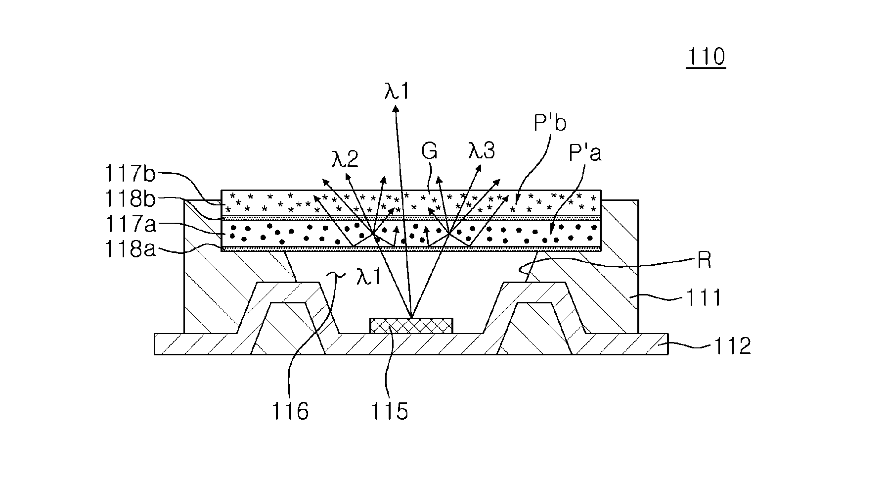
[0144]In this case, a mixing ratio (weight ratio) between the silicate phosphor and the ZnO—BaO—SiO2—P2O5—B2O3-based glass composition was set to 1:20, and a light emitting device package was prepared by directly attaching a wavelength conversion unit to an upper surface of the semiconductor LED chip (the flipchip structure illustrated in FIG. 5).
[0145]First, the light emitting device package was manufactured and color coordinates thereof were measured without an application of an optical filter. Thereafter, a first optical filter (having a cutoff wavelength of approximately 500 nm) was applied, and changed color coordinates were measured. ...
PUM
 Abstract
Description
Claims
Application Information