Wiring board and light emitting device

a light-emitting device and wiring board technology, applied in the direction of solid-state devices, printed circuit aspects, non-metallic protective coating applications, etc., can solve the problems of low adhesion strength between the adhesive agent (die-bonding material) for fixing the light-emitting elements and the reflecting layer in the lighting module, and the light-emitting elements are apt to be separated from the reflecting layer, so as to achieve the effect of improving the adhesion strength between the reflecting layer

Active Publication Date: 2014-09-18
SHINKO ELECTRIC IND CO LTD
View PDF8 Cites 26 Cited by
  • Summary
  • Abstract
  • Description
  • Claims
  • Application Information

AI Technical Summary

Benefits of technology

[0008]According to one of aspects of the present embodiment, it is possible to obtain an effect that adhesive strength between a reflecting layer and an adhesive agent can be improved when the adhesive agent is used to bond a light emitting element to the reflecting layer.

Problems solved by technology

However, from diligent studies of the present inventors, it has been obvious that adhesive strength between the adhesive agent (die bonding material) for fixing the light emitting elements and the reflecting layer is low in the lighting module.
Accordingly, when the adhesive agent is used to bond the light emitting elements to such a reflecting layer, there is a problem in that the light emitting elements are apt to be separated from the reflecting layer.

Method used


Image

  • Wiring board and light emitting device
  • Wiring board and light emitting device
  • Wiring board and light emitting device

Examples


first embodiment

[0022]A first embodiment will be described below in accordance with FIGS. 1 to 4, FIGS. 5A to 5D and FIGS. 6A to 6C.

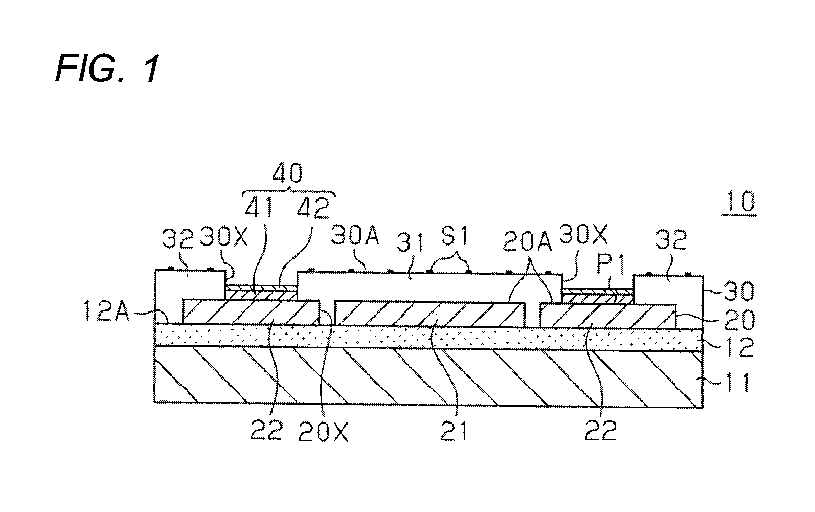
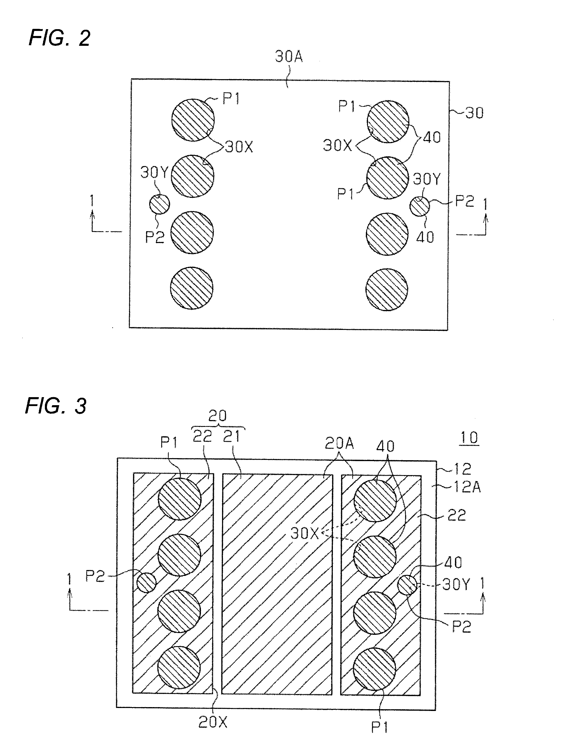
[0023]First, the structure of a wiring board 10 will be described in accordance with FIGS. 1 to 3.

[0024]As shown in FIG. 1, the wiring board 10 has a heat sink 11, an insulating layer 12 formed on the heat sink 11, wiring patterns 20 formed on the insulating layer 12, an insulating layer 30 covering a part of the wiring patterns 20, and metal layers 40 formed on the wiring patterns 20.

[0025]For example, the heat sink 11 is a flat plate substantially shaped like a rectangle in plan view. For example, copper (Cu), a Cu based alloy, iron-nickel (Fe—Ni), an Fe—Ni based alloy, aluminum (Al) or an Al based alloy etc. may be used as the material of the heat sink 11. The thickness of the heat sink 11 may be set to be, for example, about 200 to 2,000 μm.

[0026]The insulating layer 12 is formed to cover the whole of an upper surface of the heat sink 11. In other words, the heat s...

second embodiment

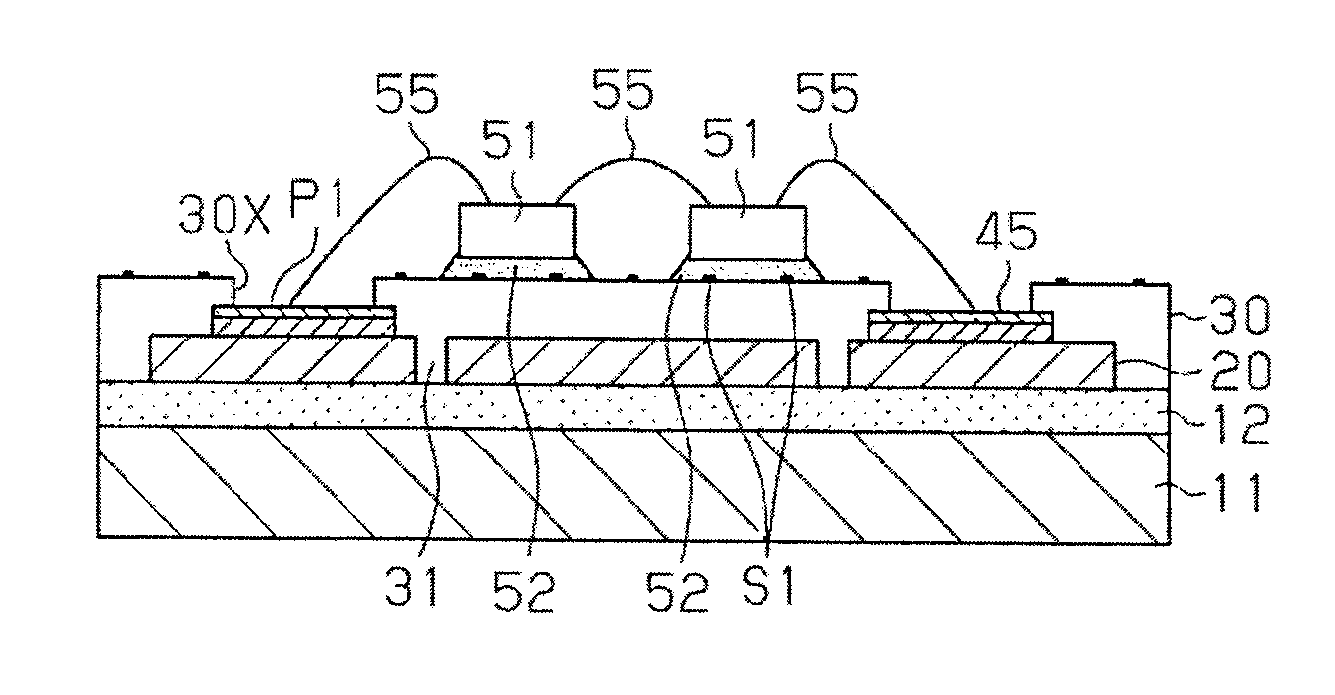
[0097]A second embodiment will be described below with reference to FIG. 10, FIGS. 11A to 11D and FIGS. 12A to 12D. Structures of an insulating layer 30 and metal layers in the embodiment are different from those in the first embodiment. Different points from the first embodiment will be described mainly.

[0098]As shown in FIG. 10, a plurality of metal layers 45 are formed on wiring patterns 20 (wiring patterns 22). Each of the metal layers 45 is substantially formed, for example, into a circular shape in plan view in the same manner as the metal layer 40. Examples of the metal layer 45 may include a metal layer in which an Ni layer and an Au layer are laminated sequentially in this order on an upper surface 20A of the wiring pattern 20, a metal layer in which an Ni layer, a Pd layer and an Au layer are laminated sequentially likewise, a metal layer in which an Ni layer, a Pd layer and an Ag layer are laminated sequentially likewise, and a metal layer in which an Ni layer, a Pd layer...


PUM


Abstract

There is provided a wiring board for mounting a light emitting element thereon. The wiring board includes: an insulating layer; a wiring pattern on the insulating layer; a reflecting layer on the insulating layer to cover the wiring pattern, wherein the light emitting element is to be mounted on a surface of the reflecting layer; and a silica film on the surface of the reflecting layer.

Description

[0001]This application claims priority from Japanese Patent Application No. 2013-052293, filed on Mar. 14, 2013, the entire contents of which are herein incorporated by reference.BACKGROUND OF THE INVENTION[0002]1. Technical Field[0003]The present disclosure relates to a wiring board and a light emitting device.[0004]2. Description of the Related Art[0005]Recently, light emitting diodes (LEDs) having low power consumption and long lives have drawn attention as light sources. For example, a lighting module mounted with a plurality of light emitting elements such as LEDs has been proposed (for example, see JP-A-2011-44593). In such a lighting module, a reflecting layer (an insulating layer) for reflecting light emitted from the mounted light emitting elements is formed in an outermost layer and the light emitting elements are mounted on the reflecting layer by an adhesive agent such as a die bonding material.[0006]However, from diligent studies of the present inventors, it has been ob...

Claims


Application Information

Patent Timeline
Patent Type & Authority Applications(United States)
IPC IPC(8): H01L33/60H05K1/02H01L33/62
CPCH01L33/60H05K1/0201H01L33/62H01L2224/48091H01L2224/48137H01L2224/73265H01L25/0753H01L2224/45144H05K3/28H05K2201/0179H05K2201/099H05K2201/2054H01L2224/45147H01L2924/181H01L24/45H01L2224/45124H01L2924/00014H01L2924/00012H01L2924/0002H01L2924/00
Inventor KOBAYASHI, KAZUTAKAHORIKAWA, YASUYOSHIAIZAWA, MITSUHIROHARA, KOJI
Owner SHINKO ELECTRIC IND CO LTD
Why Eureka
Try Eureka