

Power overlay structure and method of making same
- Summary
- Abstract
- Description
- Claims
- Application Information
AI Technical Summary
Benefits of technology
Problems solved by technology
Method used
Image

Examples
Embodiment Construction
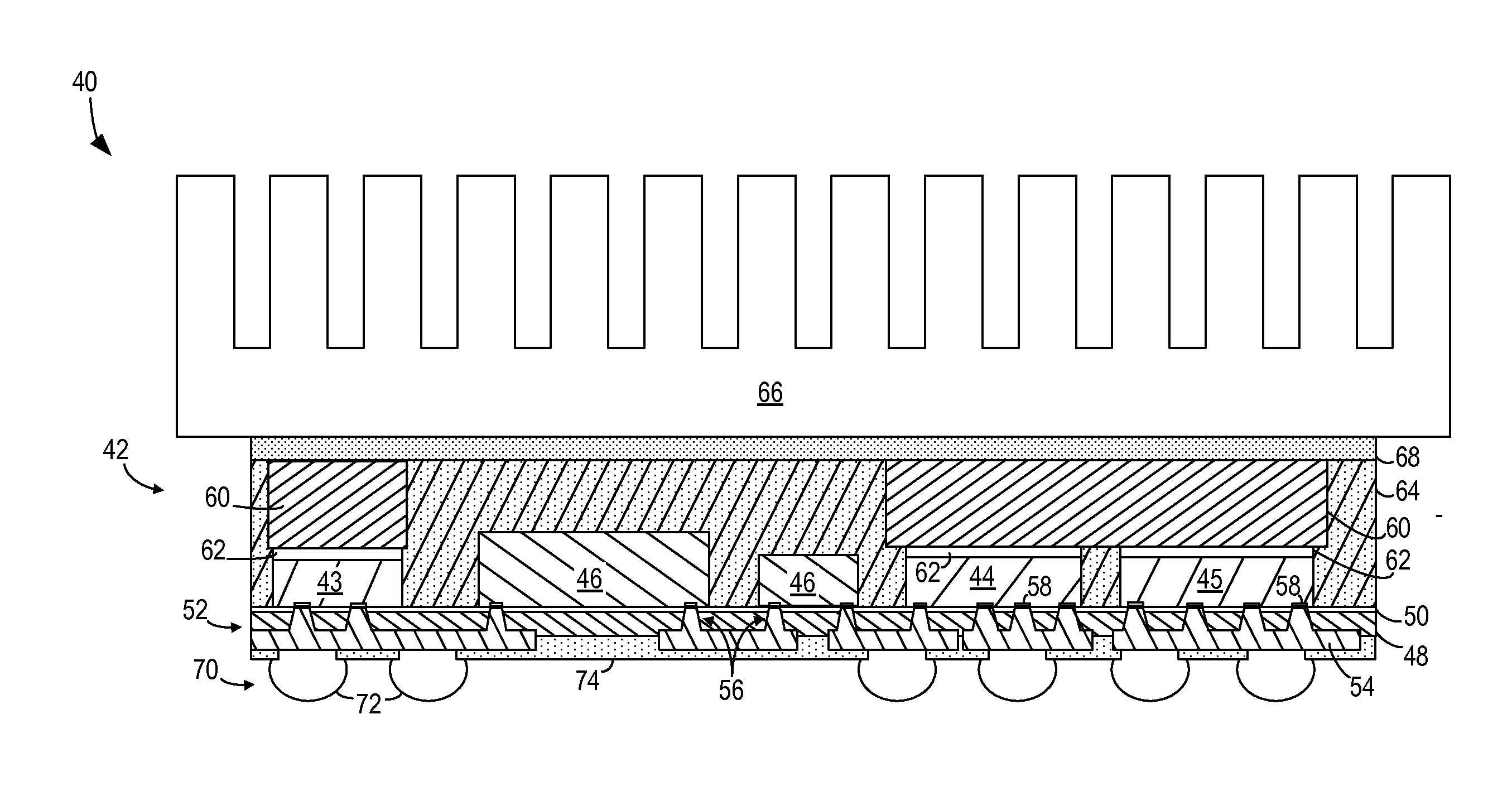
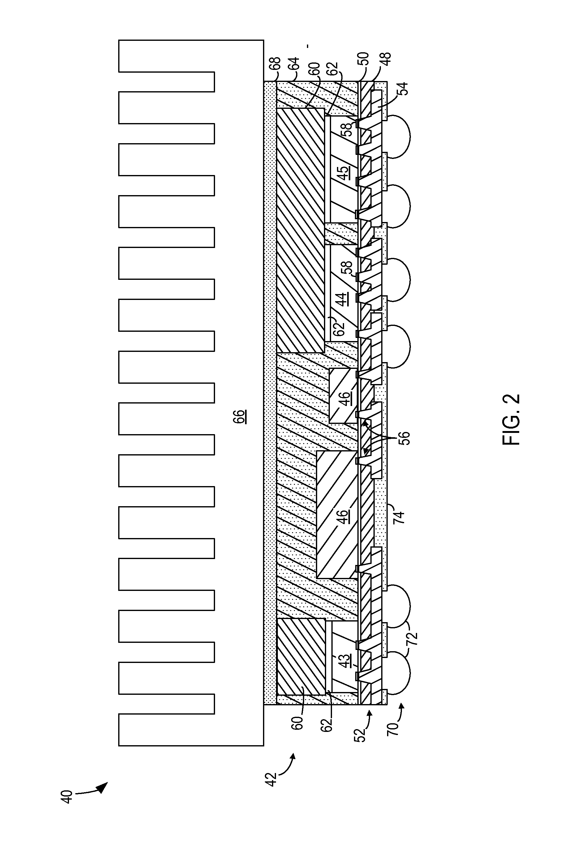
[0030]Embodiments of the present invention provide for a power overlay (POL) structure having an improved thermal interface included therein, as well as a method of forming such a POL structure. The POL structure includes conducting shims that account for semiconductor devices of varying heights and a thermal interface layer that increases options for encapsulation materials and methods.
[0031]Referring to FIG. 2, a semiconductor device assembly or power overlay (POL) structure 40 is shown according to an embodiment of the invention. POL structure 40 includes a POL sub-module 42 having one or more semiconductor devices 43, 44, 45 therein that, according to various embodiments, may be in the form of a die, diode, or other power electric device. As shown in FIG. 2, three semiconductor devices 43, 44, 45 are provided in POL sub-module 42, however, it is recognized that a greater or lesser number of semiconductor devices 43, 44, 45 could be included in POL sub-module 42. In addition to s...
PUM
 Abstract
Description
Claims
Application Information