Low-power interface and method of operation

a low-power interface and low-power technology, applied in the field of electronic devices, can solve the problems of slow mobile device performance, low power consumption, and difficulty in achieving both fast operation of the processor and low-power operation of the high-speed interface, and achieve the effects of fast processor operation, low latency, and fast performan

Active Publication Date: 2014-09-18
QUALCOMM INC
View PDF9 Cites 2 Cited by
  • Summary
  • Abstract
  • Description
  • Claims
  • Application Information

AI Technical Summary

Benefits of technology

[0004]To enable fast performance, a processor may access instructions stored “off-chip” at a memory via a high-speed interface, such as a low-power double data rate (LPDDR) interface. Because the input signals may be of a high voltage that generally should not be applied directly to core circuitry (e.g., due to potential damage to the core circuitry), the input signals may be shifted from a first (e.g., input / output or “pad”) voltage level to a second (e.g., “core”) voltage level by the high-speed interface. The high-speed interface may include multiple input receivers to receive and level-shift the input signals. Because the input receivers are associated with high power consumption, it may be efficient to disconnect or “turn off” the input receivers when data is not being written to or read from the memory. In addition, the input receivers should activate or “wake up” quickly in response to the input signals (i.e., the input receivers should be associated with low latency), which may be difficult if the input receivers are turned off when the input signals are received. Accordingly, designing a power-efficient high-speed interface while achieving low latency poses design challenges, since it may be difficult to achieve both fast operation of the processor and low-power operation of the high-speed interface.
[0005]In at least one embodiment, the high-speed interface includes an input receiver that deactivates or “powers down” by disconnecting an output load of the input receiver when data is not being written to or read from the memory. The output load may be disconnected instead of disconnecting an input node (e.g., an analog input node or a bias source) of the input receiver. Because the input node may be tied to multiple input receivers of the high-speed interface, the input node may have a high capacitance and may take a relatively long time to “settle” in response to input signals. Such a high capacitance may also make the high-speed interface slow to turn off after detecting that the input signals are not being received at the high-speed interface. By disconnecting the output load instead of the bias source, the time for “wakeup” is reduced.
[0011]One particular advantage provided by at least one of the disclosed embodiments is that an input receiver of a high-speed interface may be deactivated rapidly when input signals are not being applied to the input receiver. For example, by disconnecting an output load of the input receiver instead of disconnecting an input node of the input receiver, a “discharge” duration (e.g., a time duration during which a parasitic capacitive voltage at the input node is discharged) may be avoided. Further, by clamping or “equalizing” a voltage at the output node in response to disconnecting the output load, spurious signals at the output node can be reduced or avoided, thus protecting core circuitry that may otherwise be damaged by such spurious signals. In at least one embodiment, the input receiver is “woken up” while the output node is still charged by an “equalized” voltage, reducing or avoiding a latency caused by capacitive charging of the input node. Other aspects, advantages, and features of the present disclosure will become apparent after review of the entire application, including the following sections: Brief Description of the Drawings, Detailed Description, and the Claims.

Problems solved by technology

Increasingly, users expect electronic devices to provide fast performance while also consuming low power (e.g., having long battery life).
However, conserving battery life in this manner slows performance of the mobile devices.
In addition, the input receivers should activate or “wake up” quickly in response to the input signals (i.e., the input receivers should be associated with low latency), which may be difficult if the input receivers are turned off when the input signals are received.
Accordingly, designing a power-efficient high-speed interface while achieving low latency poses design challenges, since it may be difficult to achieve both fast operation of the processor and low-power operation of the high-speed interface.
Because the input node may be tied to multiple input receivers of the high-speed interface, the input node may have a high capacitance and may take a relatively long time to “settle” in response to input signals.
Such a high capacitance may also make the high-speed interface slow to turn off after detecting that the input signals are not being received at the high-speed interface.
As an example, because disconnecting the output load instead of the input node may potentially result in a spurious voltage at the output node, protection circuitry is used to limit the output voltage from exceeding a threshold (e.g., from reaching a voltage level that could damage core circuitry).
In at least one embodiment, the protection circuitry restricts the voltage at the output node from exceeding or reaching a pad voltage level, which could damage core circuitry components.

Method used


Image

  • Low-power interface and method of operation
  • Low-power interface and method of operation
  • Low-power interface and method of operation

Examples


Embodiment Construction

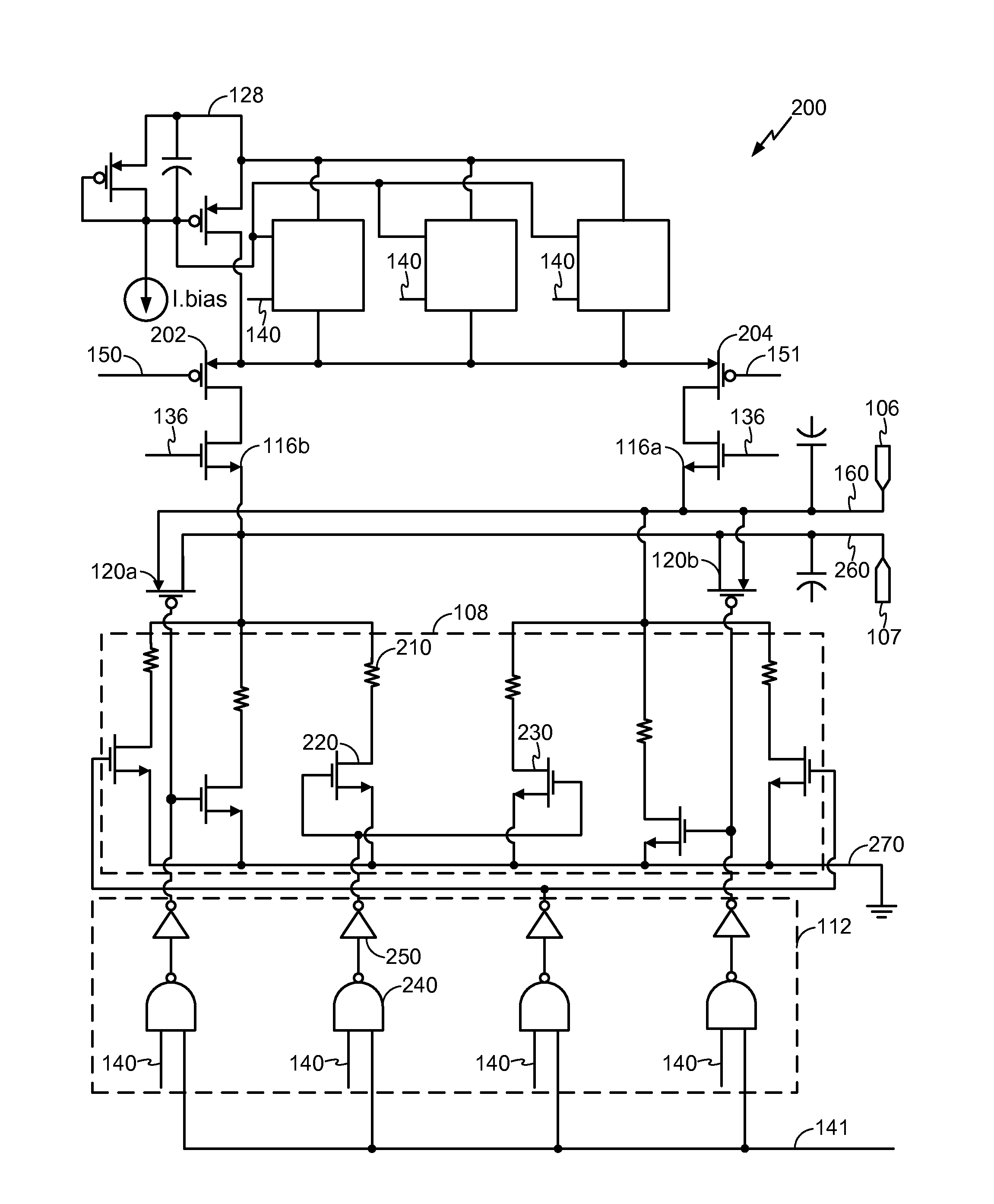
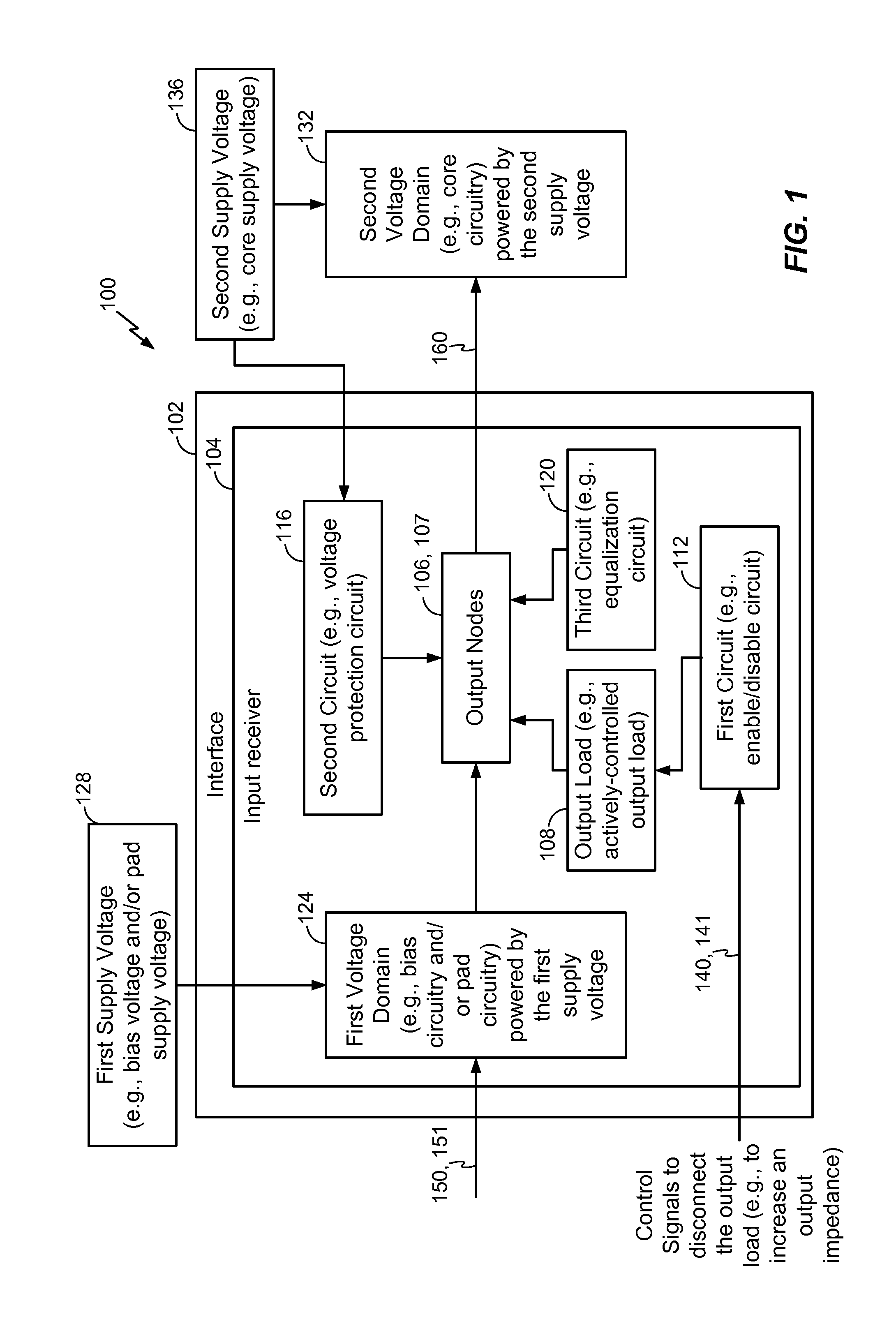
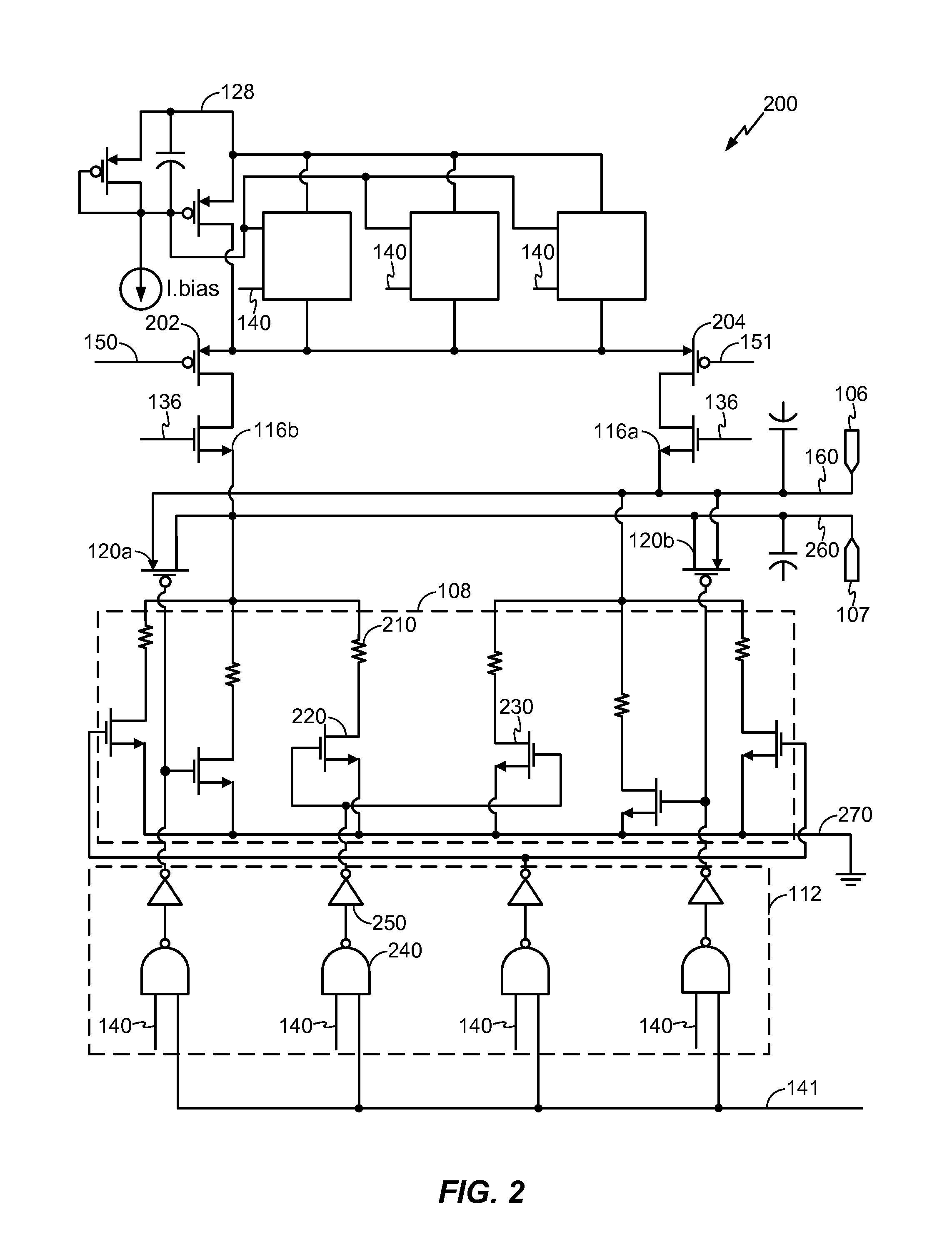
[0017]Referring to FIG. 1, a particular illustrative embodiment of a device is depicted and generally designated 100. The device 100 includes an interface 102. The interface 102 includes an input receiver 104. The input receiver 104 includes an output load 108, a first output node 106, and a second output node 107. The first output node 106 is configured to generate a first output voltage 160. In a particular embodiment, the output nodes 106, 107 correspond to a differential pair of output nodes configured to generate differential output voltages.

[0018]The device 100 further includes a first circuit 112 (e.g., an enable / disable circuit configured to enable / disable the output load 108), a second circuit 116 (e.g., a voltage protection circuit to restrict the first output voltage 160 from reaching or exceeding a threshold), and a third circuit 120 (e.g., an equalization circuit configured to equalize at least the first output voltage 160 when the output load 108 is disconnected). The ...


PUM


Abstract

In a particular embodiment, a method includes modifying an output impedance associated with the input receiver. In response to modifying the output impedance, the method restricts an output voltage at an output node of the input receiver. Particular embodiments of an input receiver circuit are also disclosed.

Description

I. FIELD[0001]The present disclosure is generally related to electronic devices and more particularly to electronic device interfaces.II. DESCRIPTION OF RELATED ART[0002]Advances in technology have resulted in smaller and more powerful electronic devices. For example, there currently exist a variety of mobile devices, such as wireless telephones, personal digital assistants (PDAs), and paging devices. The mobile devices may be small, lightweight, and easily carried by users. Wireless telephones, such as cellular telephones and Internet Protocol (IP) telephones, can communicate voice and data packets over wireless networks. Further, many such wireless telephones include other types of devices that are incorporated therein. For example, a wireless telephone can also include a digital still camera, a digital video camera, a digital recorder, and an audio file player. Also, such wireless telephones can process executable instructions, including software applications, such as a web brows...

Claims


Application Information

Patent Timeline
Patent Type & Authority Applications(United States)
IPC IPC(8): G05F1/59
CPCG05F1/59G11C7/1084
Inventor KWON, CHANG KICHEN, WILSON JIANBOJALILIZEINALI, REZA
Owner QUALCOMM INC
Why Eureka
Try Eureka