Method and apparatus for implementing wide data range and wide common-mode receivers

a receiver and data range technology, applied in the field of sense amplifiers, can solve the problems of increased overall area, insufficient voltage headroom of receiver structures, and increased implementation costs

Active Publication Date: 2014-09-18
LATTICE SEMICON CORP
View PDF5 Cites 11 Cited by
  • Summary
  • Abstract
  • Description
  • Claims
  • Application Information

AI Technical Summary

Benefits of technology

[0022]In one embodiment, the method may include controlling a degree of change in the output voltage caused by the sensing circuit using a sensing current control circuit. The method may also include controlling a degree of amplification of the changed output voltage caused by the regeneration circuit using a regeneration current control circuit. The method may also include changing the output voltage at the output node ...

Problems solved by technology

This results in an increased overall area and, hence, cost of implementation.
Moreover, many receiver structures suffer from insufficient voltage headroom because of low supply voltages used in advanced fabrication processes.
As a result, these receiver structures operate with ...

Method used


Image

  • Method and apparatus for implementing wide data range and wide common-mode receivers
  • Method and apparatus for implementing wide data range and wide common-mode receivers
  • Method and apparatus for implementing wide data range and wide common-mode receivers

Examples


example circuit

Architecture

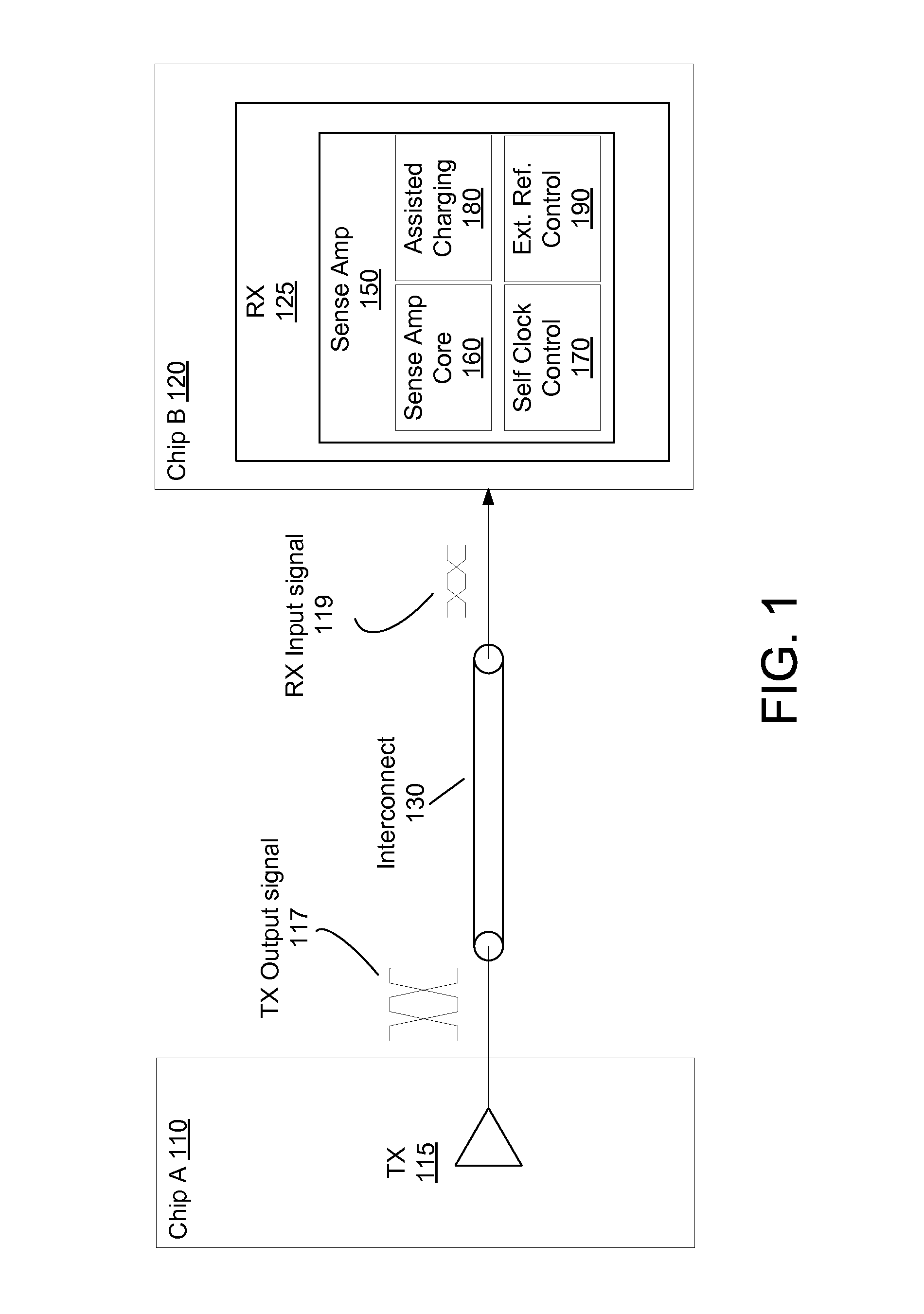
[0050]FIG. 1 is a diagram illustrating a chip-to-chip interface between two chips, according to one embodiment. Chip A 110 includes a transmitter (TX) 115 to transmit signals over an interconnect 130 to chip B 120 with a receiver (RX) 125. The TX 115 generates TX output signal 117 at an output of the transmitter 115 to drive the interconnect 130 and the RX 125. However, RX input signal 119 received at an input of the receiver 125 is degraded, because of non-idealities such as (i) parasitics in the interconnect, off chip components, bonding wires, and bonding pads, (ii) impedance mismatch, (ii) cross talks, and (iv) external noise. The receiver 125 employs a sense amplifier 150 as a front end of the receiver 125, and amplifies the input signal 119 to a proper level. The amplified signal enables logic operation or process to be performed on and / or off the chip B 120.

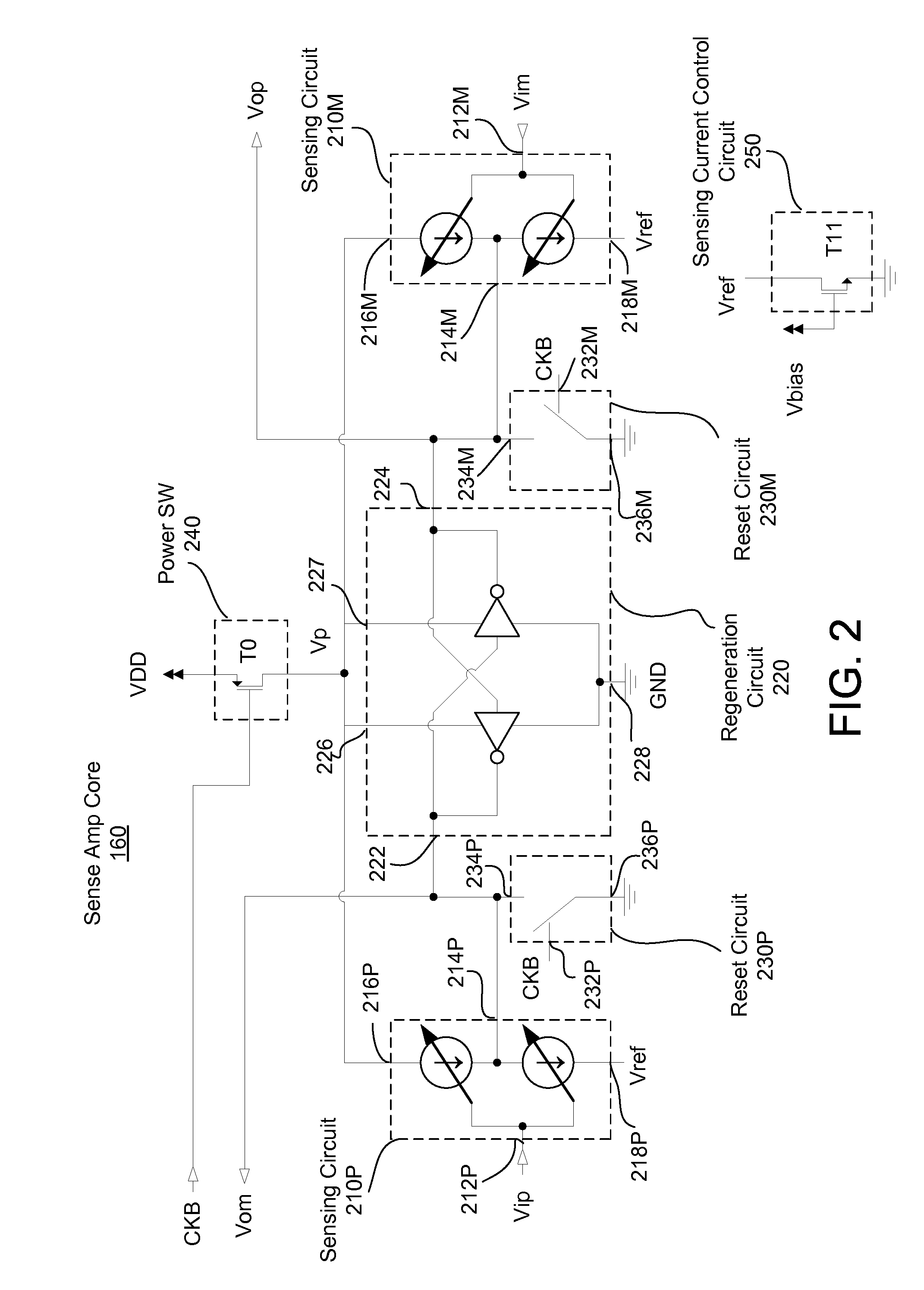
[0051]The sense amplifier 150 includes, among other components, a sense amplifier core circuit 160. The sens...

example configuration

and Operation of Sense Amplifier

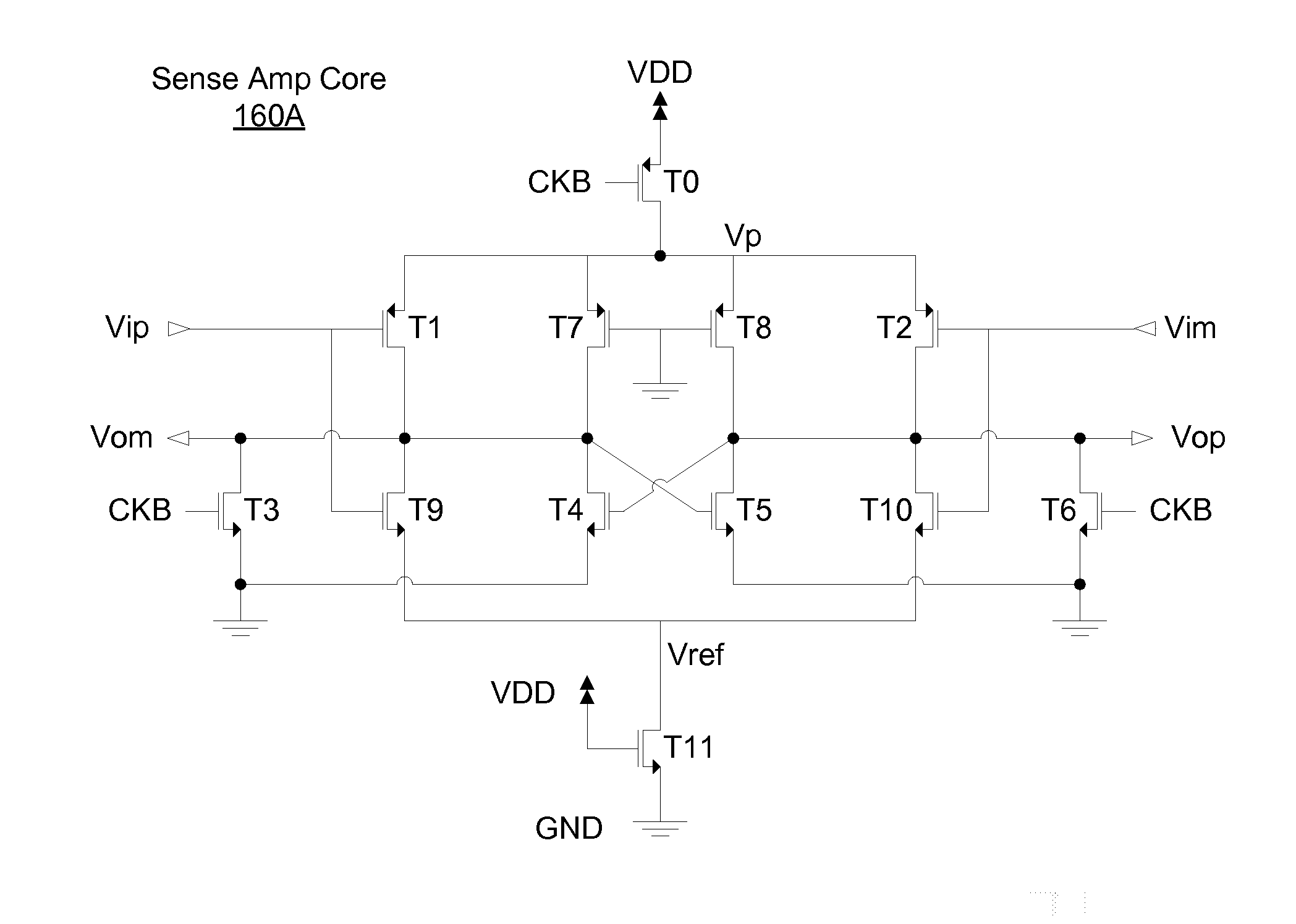
[0074]Referring to FIG. 5, illustrated is an example embodiment of a sense amplifier core circuit 160A. The configuration and operation of the embodiment of FIG. 5 is substantially the same as the embodiment of FIG. 2 except that the positive input sensing circuit 210P is replaced with the sensing circuit 210A, the negative input sensing circuit 210N is replaced with the sensing circuit 210A, and the regeneration control bias Vb is coupled to GND.

[0075]The sensing circuit 210A includes the NMOS transistor T1 and the PMOS transistor T9, where the bias node Vbias of the NMOS transistor T11 is coupled to VDD. Similarly, the sensing circuit 210A comprises a NMOS transistor T2 and the PMOS transistor T10. In addition, the back-to-back pseudo inverters in the regeneration circuit 220B are employed as the regeneration circuit 220 in FIG. 2.

[0076]FIG. 6 is a timing diagram illustrating an example operation of the sense amplifier in FIG. 5, according to one em...


PUM


Abstract

Embodiments of disclosed configurations include a circuit and system for a sense amplifier having a sensing circuit changing an output voltage at an output node based on a time that is defined by the output voltage reaching a threshold voltage level. The sensing circuit changes the output voltage at the output node before the time. In addition, a regeneration circuit amplifies the changed output voltage at the time. The sense amplifier offers sufficient voltage headroom to improve operation speed and power efficiency.

Description

CROSS-REFERENCE TO RELATED APPLICATION[0001]This application claims priority under 35 U.S.C. §119(e) to co-pending U.S. Provisional Patent Application No. 61 / 801,605 filed on Mar. 15, 2013, which is incorporated by reference herein in their entirety.BACKGROUND[0002]1. Field of Art[0003]This disclosure generally relates to wired communications in electronic devices and, more particularly, to a sense amplifier implemented in a receiving device.[0004]2. Description of the Related Art[0005]Many electronic systems include integrated circuits (chips) that communicate with each other. For example in a computer, integrated circuits such as a dynamic random access memory (DRAM) communicate with a central processing unit (CPU), and graphics processing unit (GPU). To enable communication between two or more different integrated circuits, a transmitter in one integrated circuit transmits signals to a receiver in another integrated circuit via an interconnect.[0006]Generally, a receiver structur...

Claims


Application Information

Patent Timeline
IPC IPC(8): H03F3/16
CPCH03F3/16G11C7/062G11C7/08H03F3/45264G11C7/065
Inventor TALEGAONKAR, MRUNMAYGONDI, SRIKANTH
Owner LATTICE SEMICON CORP
Why Eureka
Try Eureka