Neural sensing device and method for making the same

a neural sensing and noise reduction technology, applied in the field of neurological diagnostic and therapeutic medical devices, can solve the problems that the conventional neural sensing devices are affected by undesired noise, and achieve the effect of reducing nois

Active Publication Date: 2014-09-18
ADVANCED SEMICON ENG INC
View PDF8 Cites 7 Cited by
  • Summary
  • Abstract
  • Description
  • Claims
  • Application Information

AI Technical Summary

Benefits of technology

[0007]The integrated circuit portion comprises at least one electrical element, a plurality of metal layers and at least one dielectric layer, the at least one electrical element is disposed adjacent to the active surface of the base and covered by the dielectric layer, and the metal layers are embedded in the dielectric layer. Each of the microprobes has a probe body and an isolation layer, wherein the probe body protrudes from the backside surface of the base, the conductive via penetrates through the probe body, and the isolation layer covers the probe body and has an opening to expose a tip of the conductive via. The exposed tip can be plated with platinum which is considered safe for humans. In operation, the microprobes are used to penetrate the stratum germinativum layer of human skin to collect bio-signals via the exposed tips of the conductive vias. When the stratum germinativum layer is penetrated, the microprobes are electrically insulated from the stratum corneum layer of the skin by the isolation layer, thus reducing noise.

Problems solved by technology

Unfortunately, conventional neural sensing devices tend to be affected by undesired noise through the portions of the microprobes in the stratum corneum.

Method used


Image

  • Neural sensing device and method for making the same
  • Neural sensing device and method for making the same
  • Neural sensing device and method for making the same

Examples


Embodiment Construction

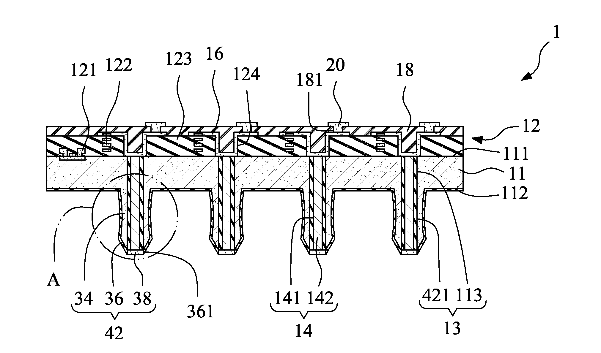
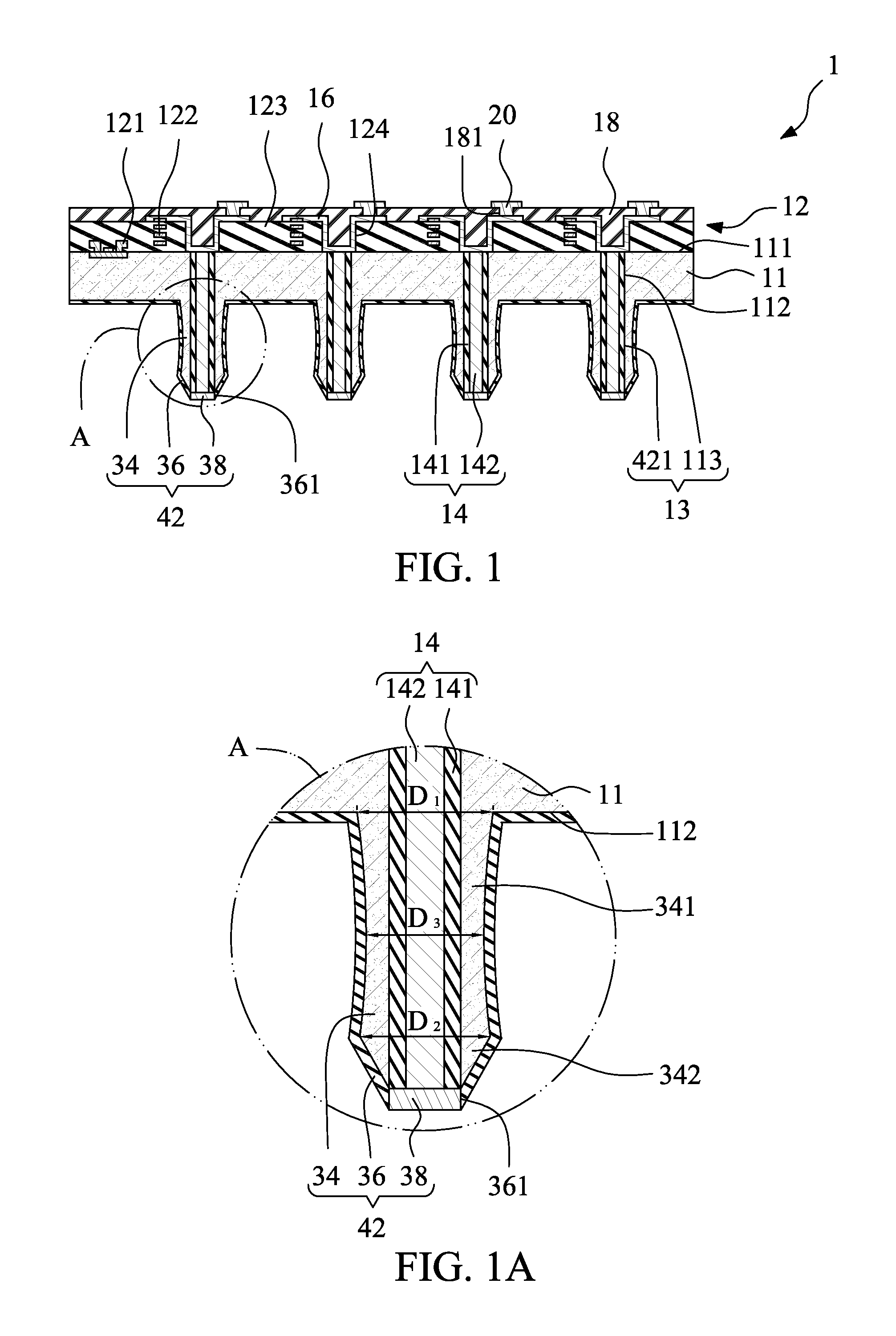
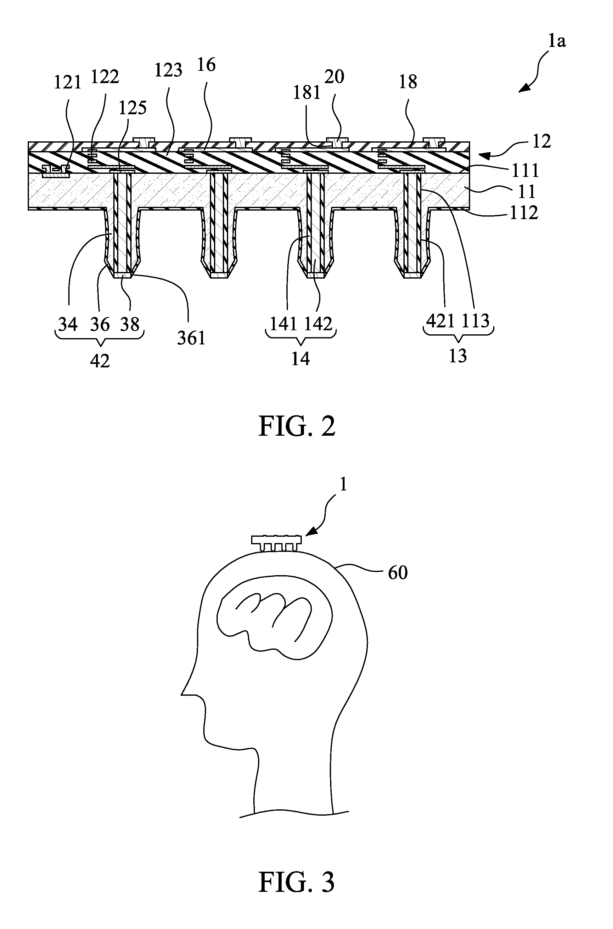
[0020]Referring to FIG. 1, a cross sectional view of a neural sensing device 1, according to an embodiment of the present invention, is illustrated. The neural sensing device 1 comprises a base 11, an integrated circuit portion 12, a plurality of conductive vias 14, a plurality of redistribution layers 16, a protection layer 18, a plurality of under bump metallurgies (UBMs) 20 and a plurality of microprobes 42.

[0021]The base 11 has an active surface 111, a backside surface 112 and a plurality of base holes 113. In this embodiment, the material of the base 11 is silicon.

[0022]The integrated circuit portion 12 is disposed on the active surface 111 of the base 11. In this embodiment, the integrated circuit portion 12 comprises at least one electrical element 121, a plurality of metal layers 122, at least one dielectric layer 123, and a plurality of openings 124.

[0023]The at least one electrical element 121 (which can include complementary metal-oxide-semiconductor (CMOS), micro-electro...


PUM


Abstract

The present invention provides a neural sensing device and method for making the same. The neural sensing device includes a base, an integrated circuit portion and a plurality of microprobes. The base has an active surface and a backside surface. The integrated circuit portion is disposed on the active surface of the base. The microprobes protrude from the backside surface of the base. The conductive vias are disposed in the microprobes and electrically connected to the integrated circuit portion.

Description

BACKGROUND OF THE INVENTION[0001]1. Field of the Invention[0002]The present invention relates to neurological diagnostic and therapeutic medical devices, and, more particularly, to a neural sensing device with a plurality of microprobes useful for collecting bio-electrical signals and a method for making the same.[0003]2. Description of the Related Art[0004]Conventional neural sensing devices for use in recording and measuring electrical activity of the brain, such as those used in electroencephalography (EEG), include a plurality of microprobes, each having a metal needle or a needle coated with a metal layer. The microprobes are utilized to penetrate the skin of the scalp to collect bio-electrical signals from a patient.[0005]Skin is a layered structure, including two primary layers: the epidermis, which provides waterproofing and serves as a barrier to infection; and the dermis, which serves as a location for the appendages of the skin. The epidermis can be roughly divided into a...

Claims


Application Information

Patent Timeline
Patent Type & Authority Applications(United States)
IPC IPC(8): A61B5/04H01L21/768
CPCH01L21/76898A61B5/04001A61B5/685A61B2562/12A61B5/24H01L21/6835H01L21/6836H01L23/481H01L24/02H01L24/03H01L24/05H01L24/92H01L24/94H01L2221/68327H01L2221/6834H01L2224/0231H01L2224/0235H01L2224/02372H01L2224/05569H01L2224/92H01L2224/94H01L2924/00012H01L2224/03H01L2221/68304H01L21/304H01L21/56H01L2221/68381H01L21/78H01L2924/00014A61B5/6868A61B2562/046A61B5/291
Inventor CHEN, KUO-HUA
Owner ADVANCED SEMICON ENG INC
Why Eureka
Try Eureka