Supercharge Your Innovation With Domain-Expert AI Agents!

Liquid crystal display

Inactive Publication Date: 2014-09-25
HANNSTAR DISPLAY CORPORATION
View PDF4 Cites 11 Cited by
  • Summary
  • Abstract
  • Description
  • Claims
  • Application Information

AI Technical Summary

Benefits of technology

The present invention is a liquid crystal display with a common electrode below the pixel electrode to prevent capacitor coupling. This allows for a larger pixel size and a higher pixel opening ratio. Bumps on the electrodes enable liquid crystal molecules to arrange vertically, improving response time. These features make the display more efficient and effective.

Problems solved by technology

However, the researcher may meet the problem that the pixel opening ratio (also called “pixel aperture rate” or Pixel AR) will become lower when developing liquid crystal display with high PPI (Pixel per Inch) or with high pixel density.
Therefore, it is still an important issue to design liquid crystal displays with both high pixel density and high pixel opening ratio.

Method used


Image

  • Liquid crystal display
  • Liquid crystal display
  • Liquid crystal display

Examples


first embodiment

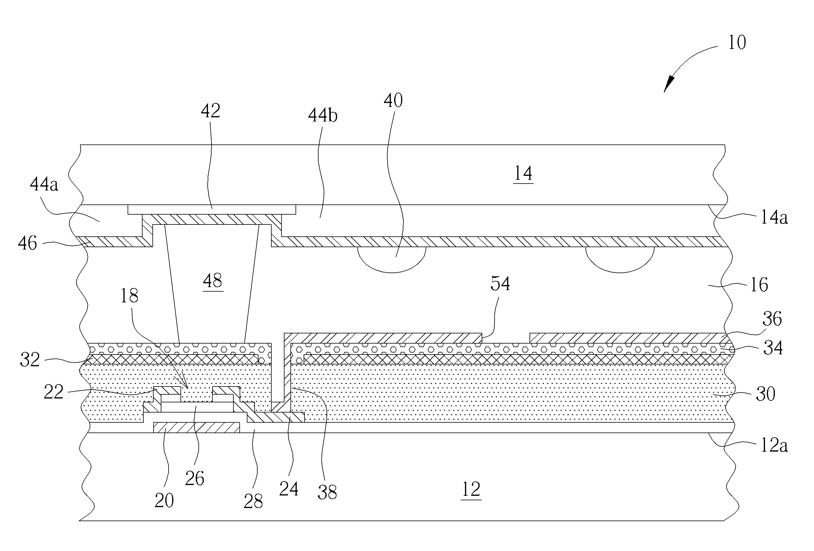
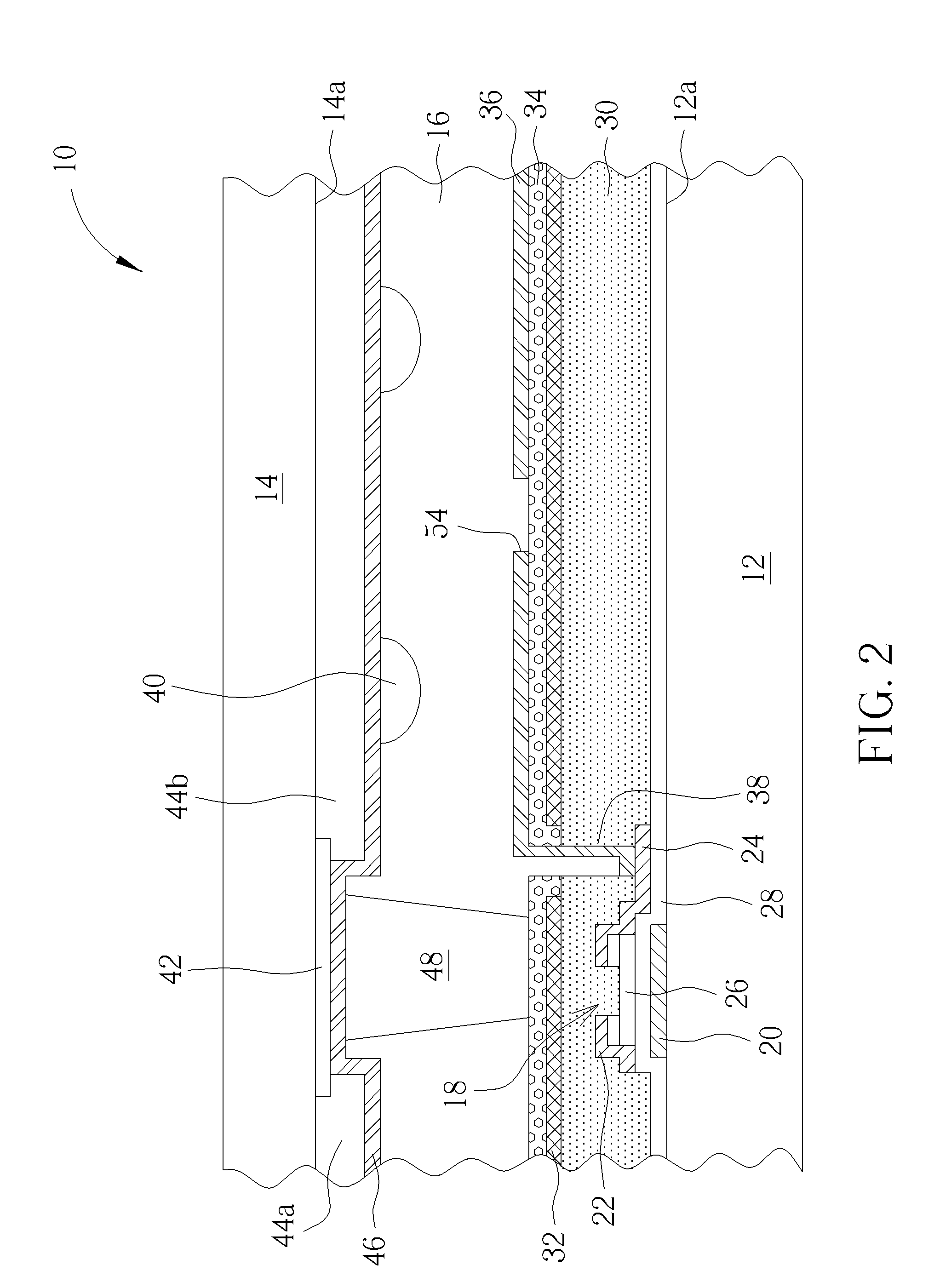
[0017]Referring to FIG. 1 and FIG. 2, FIG. 1 is a schematic top-view diagram according to the present invention liquid crystal display and FIG. 2 is a schematic sectional view of the liquid crystal display along the sectional line A-A shown in FIG. 1. The present invention liquid crystal display 10 includes a first substrate 12, a second substrate 14 and a liquid crystal layer 16, wherein the first substrate 12 is disposed below the second substrate 14 and the liquid crystal layer 16 is disposed between the first substrate 12 and the second substrate 14. At least one TFT 18 is disposed on the upper surface 12a of the first substrate 12, including a gate 20, a source 22, a drain 24 and a semiconductor layer 26. In this embodiment, the present invention liquid crystal display 10 may include a plurality of TFTs 18, while FIG. 1 and FIG. 2 illustrate only one TFT 18 for explanation. Furthermore, a gate insulating layer 28 is disposed between the semiconductor layer 26 and the gate 20. T...

fourth embodiment

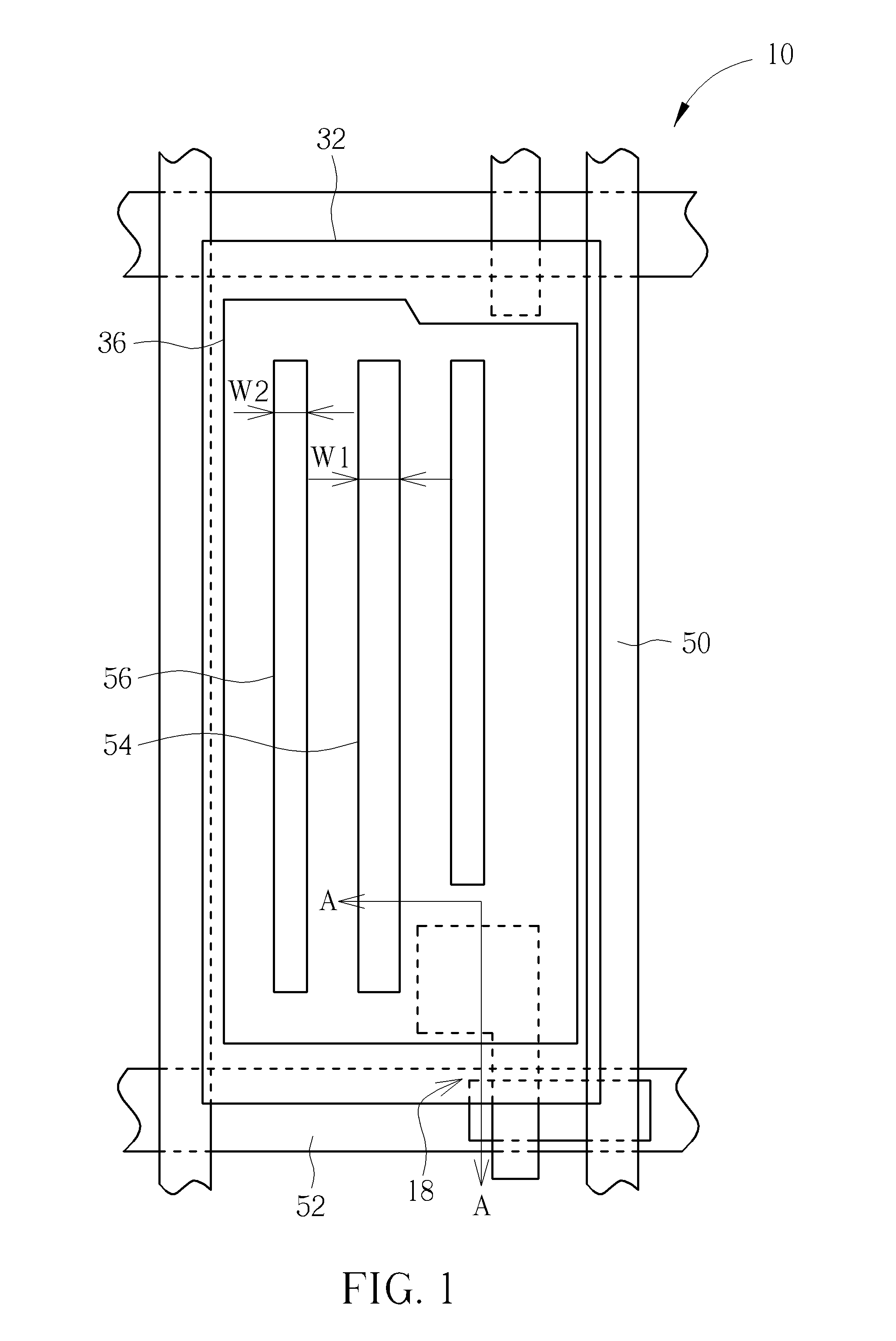
[0025]Referring to FIG. 5, FIG. 5 is a schematic sectional view according to the present invention liquid crystal display. In contrast to the previous embodiment, the pixel electrode 36 in this embodiment includes a plurality of slits 56 and at least one main slit 54, wherein the width W1 of the main slit 54 is greater than the width W2 of slits 56. Furthermore, the common electrode 32 includes at least one opening 58 corresponding to the portion of the pixel electrode 36 without the slits 56 and the main slit(s) 54, for instance. By disposing the openings 58, the area of the common electrode 32 is reduced while the conductive property of the common electrode 32 is not affected, thus the storage capacitor content formed between the common electrode 32 and the pixel electrode 36 is reduced. As a result, the storage capacitor content can be adjusted by the way of disposing the openings 58 in the common electrode 32 and designing the pattern and size of the openings 58 so as to avoid i...


PUM


Abstract

A liquid crystal display includes a first substrate, a second substrate, and a liquid crystal layer, wherein the first substrate is disposed below the second substrate and the liquid crystal layer is disposed between the first substrate and the second substrates. The liquid crystal display further includes at least one thin film transistor, a common electrode, a first insulating layer, and at least one pixel electrode disposed on the upper surface of the first substrate in order. A plurality of bumps are disposed on the lower surface of the second substrate. The thin film transistor includes a gate, a source, and a drain.

Description

BACKGROUND OF THE INVENTION[0001]1. Field of the Invention[0002]The present invention is related to a liquid crystal display (LCD), and more particularly, to a liquid crystal display adopting HannStar ultra-high aperture (HUA) technology and with a plurality of bumps disposed on a side of the liquid crystal layer.[0003]2. Description of the Prior Art[0004]Liquid crystal displays have advantages of portability, low power consumption, and low radiation. Therefore, they are widely used in various portable information products, such as notebooks, personal data assistants (PDA), and have replaced cathode ray tube (CRT) monitor in desktop computers gradually.[0005]Liquid crystal molecules serve as light valves in the liquid crystal display to control the light transmittance in each pixel of each scan time period. Based on the control mechanism of the liquid crystal molecules, liquid crystal displays can be divided into vertical alignment (VA) type liquid crystal displays and plane switchi...

Claims


Application Information

Patent Timeline
IPC IPC(8): G02F1/1343
CPCG02F1/134309G02F1/133707G02F1/134363
Inventor YU, CHIA-HUALIN, SUNG-CHUNKO, CHIEN-CHUANCHANG, HSIEN-CHENGLIU, HSUAN-CHEN
Owner HANNSTAR DISPLAY CORPORATION
Features
  • R&D
  • Intellectual Property
  • Life Sciences
  • Materials
  • Tech Scout
  • Unparalleled Data Quality
  • Higher Quality Content
  • 60% Fewer Hallucinations
Learn More