System and method for drying substrates

a technology of substrates and systems, applied in the direction of basic electric elements, lighting and heating equipment, electrical equipment, etc., can solve the problems of high drying cost, long cycle time, and contamination of surface, and achieve the effect of high aspect ratio

Inactive Publication Date: 2014-10-02
JST MFG CO LTD
View PDF6 Cites 16 Cited by
  • Summary
  • Abstract
  • Description
  • Claims
  • Application Information

AI Technical Summary

Problems solved by technology

However, certain semiconductor substrates, such as those having micro-electromechanical systems (MEMS) and photovoltaics, can have deep vias and / or high aspect ratio features on the surface, which can present a particular challenge for drying.
These types of features can contain or trap water after rinsing, which can leave surface contaminants in the form of water spotting.
Water remaining on a substrate can also cause long cycle times and incomplete drying, potentially leading to stiction of MEMS devices on the substrate.
Liquid spots left on a semiconductor wafer surface can also cause oxidation that damages components on the wafer.

Method used


Image

  • System and method for drying substrates
  • System and method for drying substrates
  • System and method for drying substrates

Examples


Embodiment Construction

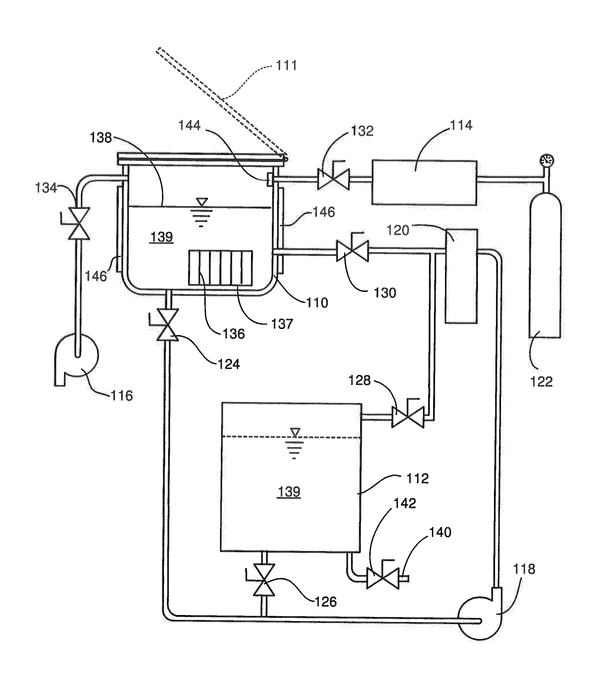
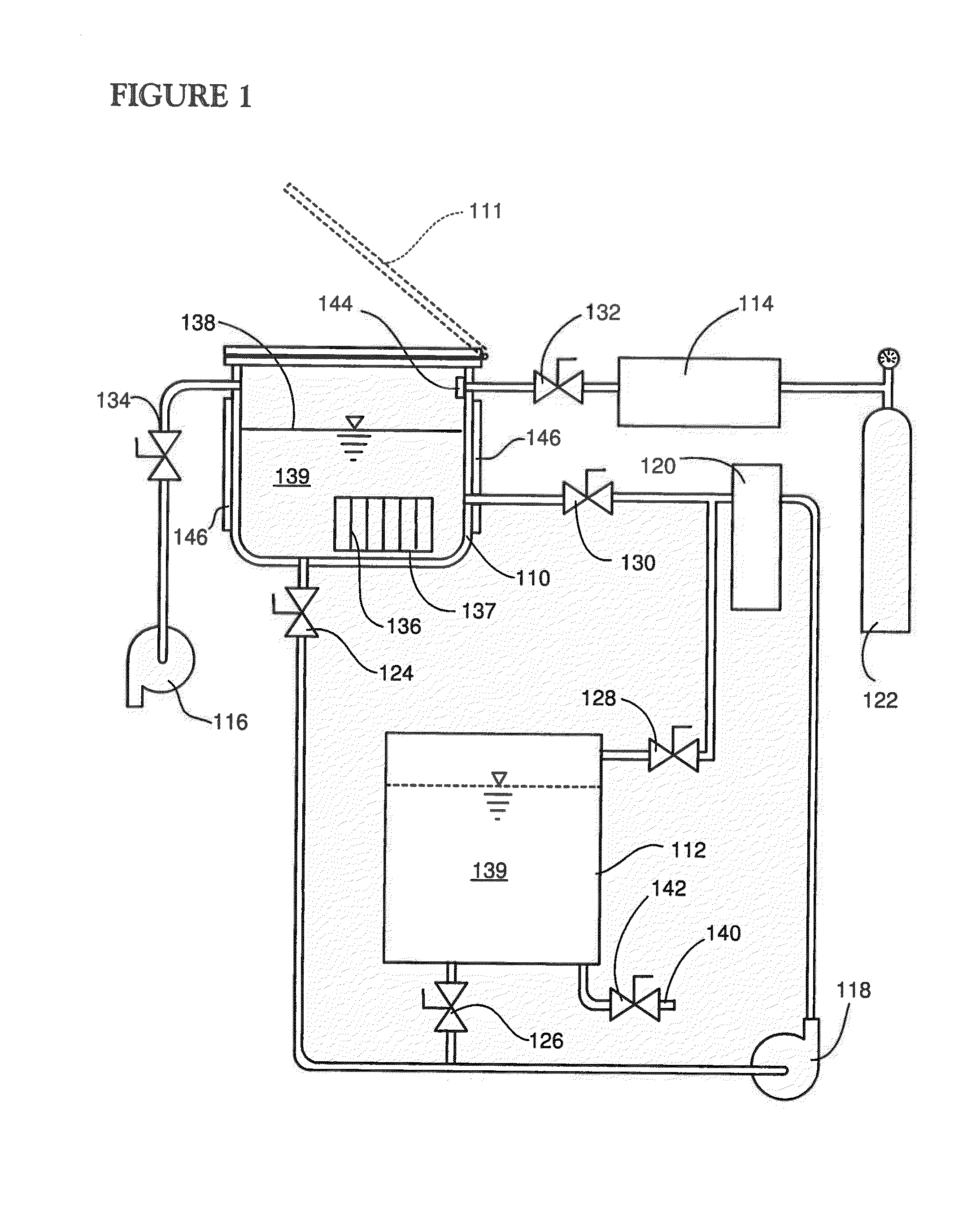
[0018]In the following description, reference is made to the accompanying drawings that form a part thereof, and in which is shown by way of illustration specific exemplary embodiments in which the invention may be practiced. These embodiments are described in sufficient detail to enable those skilled in the art to practice the invention, and it is to be understood that modifications to the various disclosed embodiments may be made, and other embodiments may be utilized, without departing from the spirit and scope of the present invention. The following detailed description is, therefore, not to be taken in a limiting sense.

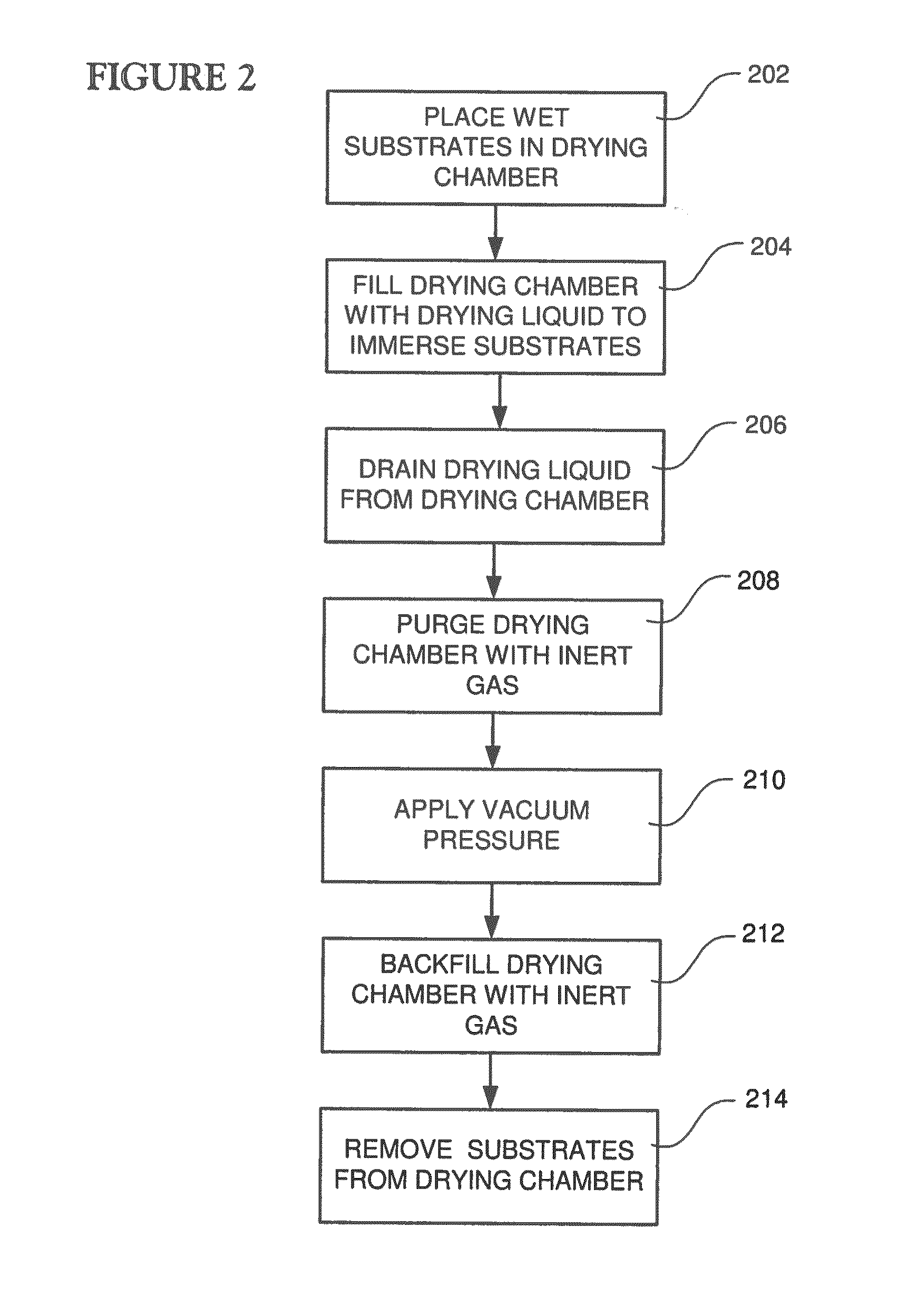
[0019]As noted above, some of the known methods for drying substrates, such as semiconductor substrates, can leave surface contaminants in the form of water spotting, and can also cause incomplete drying, potentially leading to stiction of MEMS devices on the substrate. Those of skill in the art will recognize that the term “stiction” is an informal contraction o...


PUM


Abstract

A method for drying a wet semiconductor substrate includes immersing the wet substrate in a rinsing liquid in a sealed drying chamber, producing a volume of vaporized drying fluid in a vapor generator, establishing fluid communication between the vapor generator and the drying chamber, transferring the vaporized drying fluid to the drying chamber by removing the rinsing liquid from the drying chamber, and allowing the vaporized drying fluid to condense on the wet substrate. The method further includes providing vacuum pressure within the drying chamber and backfilling the drying chamber with an inert gas to substantially achieve atmospheric pressure.

Description

PRIORITY CLAIM[0001]The present application is a continuation-in-part of U.S. patent application Ser. No. 12 / 862,703, filed on Aug. 24, 2010 and entitled SYSTEM AND METHOD FOR DRYING SUBSTRATES, the disclosure of which is incorporated herein by reference in its entirety.FIELD OF THE DISCLOSURE[0002]The present disclosure relates generally to the drying of substrates following wet processing steps. More specifically, the present disclosure relates to a system and method for drying substrates that is effective with substrates having high aspect ratio features or MEMS features that can tend to trap liquids after rinsing.BACKGROUND[0003]The semiconductor manufacturing process typically includes multiple “wet” processing steps, which can involve acids, bases, and solvents, for example. Each of these steps is frequently followed by a rinse with de-ionized (DI) water, and then drying. The drying step is often the last step that a given substrate will encounter before its next process step....

Claims


Application Information

Patent Timeline
Patent Type & Authority Applications(United States)
IPC IPC(8): F26B20/00
CPCF26B20/00H01L21/02052H01L21/67028H01L21/02057H01L21/67057H01L21/67086H01L21/67034H01L21/67051
Inventor CAMPION, DAVIDWILSON, TIMOTHYZRNO, RYAN
Owner JST MFG CO LTD
Why Eureka
Try Eureka