Semiconductor device including sti structure and fabrication method

Active Publication Date: 2014-10-02
SEMICON MFG INT (SHANGHAI) CORP
View PDF3 Cites 0 Cited by
  • Summary
  • Abstract
  • Description
  • Claims
  • Application Information

AI Technical Summary

Benefits of technology

The patent text discusses how the increase in the integration degree of ICs has led to a decrease in the width of the semiconductor substrate between neighboring shallow trench isolation structures or the channel width of formed transistors. This decrease in channel width can affect the drive current of the transistor. The text suggests that increasing the width of the active region between neighboring STI structures can help to increase the channel width of the transistor without decreasing the integration degree of ICs and increasing chip area. The technical effect of this method is to enhance the performance of transistors without adding complexity and cost to the manufacturing process.

Problems solved by technology

This may result in narrow channel effect to cause reduction of drive current of the FETs.
However, the fabrication process of such multi-gate devices is complex and with high cost.

Method used


Image

  • Semiconductor device including sti structure and fabrication method
  • Semiconductor device including sti structure and fabrication method
  • Semiconductor device including sti structure and fabrication method

Examples


Embodiment Construction

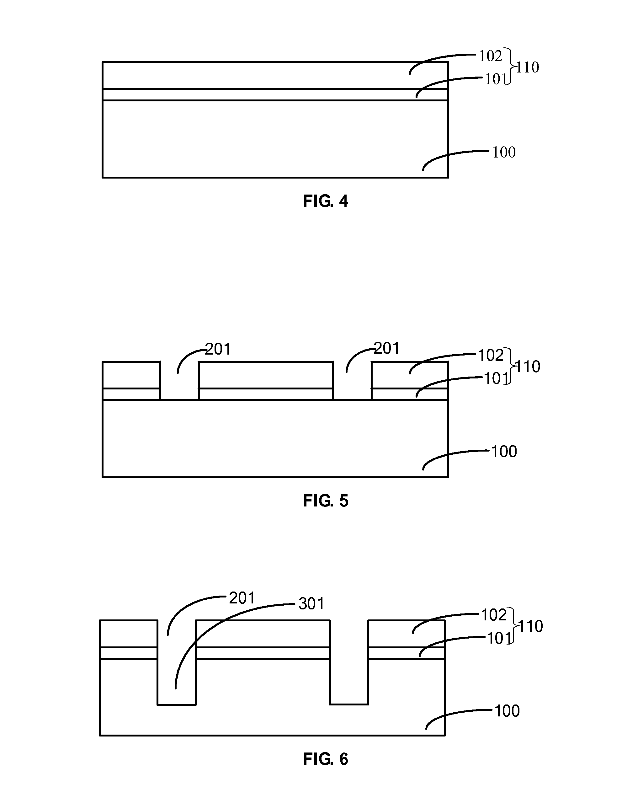
[0015]Reference will now be made in detail to exemplary embodiments of the invention, which are illustrated in the accompanying drawings. Wherever possible, the same reference numbers will be used throughout the drawings to refer to the same or like parts.

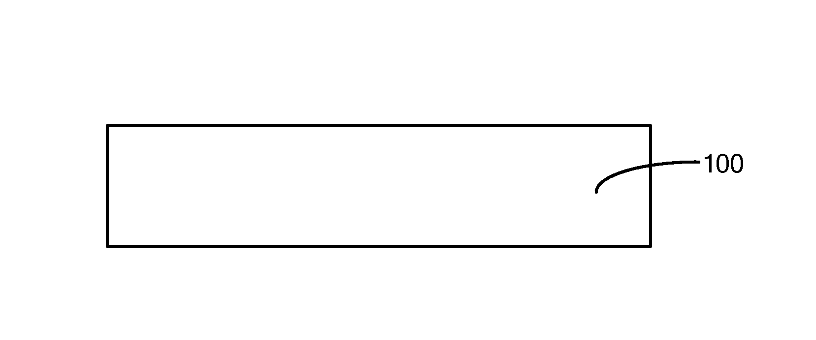
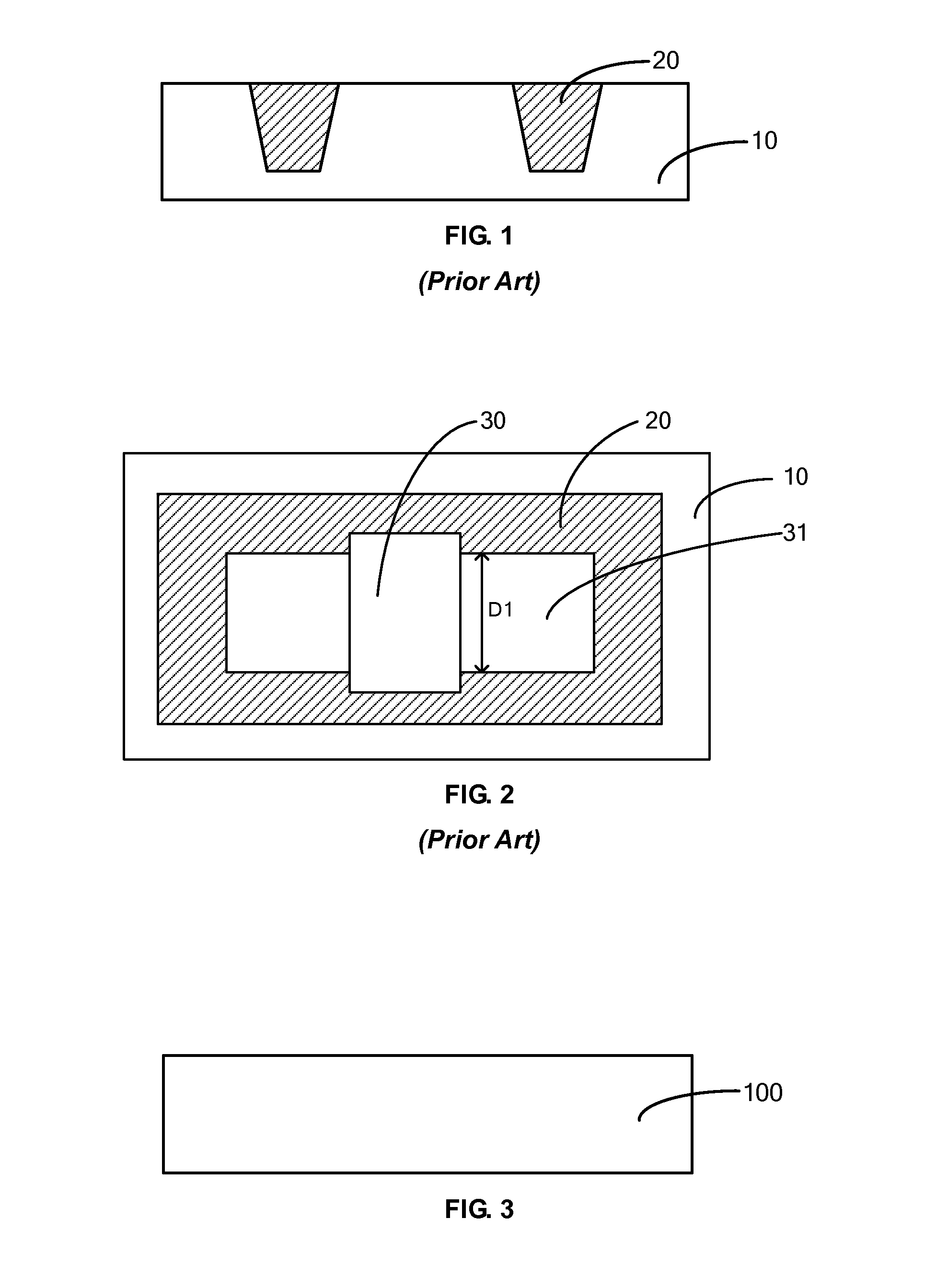
[0016]As integration degree of ICs is increasingly enhanced, width (e.g., D1 shown in FIG. 2) of semiconductor substrate between neighboring shallow trench isolation (STI) structures or channel width of formed transistor decreases. The decrease of the channel width may cause reduction of the drive current of the transistor. Although a multi-gate transistor can be employed to increase channel width of the transistor, the manufacturing process is a complex with high cost. Therefore, increasing a width of active region between neighboring STI structures can be an effective way to enhance the channel width of transistor formed in the active region. Methods for increasing a width of an active region may include increasing a distance bet...


PUM


Abstract

Semiconductor devices including STI structures and their fabrication methods are provided. A mask layer is provided on a semiconductor substrate and patterned to form an opening in the mask layer to expose a surface portion of the semiconductor substrate. A trench is then formed in the semiconductor substrate by etching along the opening. A first dielectric layer is formed in the trench and has a top surface lower than a top surface of the semiconductor substrate to provide an uncovered sidewall surface of the trench in the semiconductor substrate. An epitaxial layer is formed on the uncovered sidewall surface of the trench in the semiconductor substrate. The epitaxial layer includes a spacing to expose a surface portion of the first dielectric layer. A second dielectric layer is formed on the exposed surface portion of the first dielectric layer to fill the spacing formed in the epitaxial layer.

Description

CROSS-REFERENCES TO RELATED APPLICATIONS[0001]This application claims priority to Chinese Patent Application No. CN201310113662.5, filed on Apr. 2, 2013, the entire contents of which are incorporated herein by reference.FIELD OF THE INVENTION[0002]The present disclosure generally relates to the field of semiconductor manufacturing technology and, more particularly, relates to semiconductor devices including shallow trench isolation (STI) structures and methods for making the same.BACKGROUND[0003]With advances of semiconductor process technology and decreasing of process node, critical dimensions (CDs) of semiconductor devices are further reduced and channel widths of field-effect transistors (FETs) keep narrowing down. This may result in narrow channel effect to cause reduction of drive current of the FETs. Multi-gate devices such as Fin FETs are conventionally used to increase the channel width and thus to increase the drive current. However, the fabrication process of such multi-g...

Claims


Application Information

Patent Timeline
IPC IPC(8): H01L29/06H01L21/762
CPCH01L21/76224H01L29/0649H01L21/76232H01L29/1033H01L29/045H01L29/167H01L29/78
Inventor ZHAO, MENG
Owner SEMICON MFG INT (SHANGHAI) CORP
Why Eureka
Try Eureka