Low Power Bias Compensation Scheme Utilizing A Resistor Bias

a bias compensation and resistor bias technology, applied in the direction of power conversion systems, dc-dc conversion, oscillation generators, etc., can solve the problems of vco noise that may have a significant impact on the phase noise and time domain jitter at the output of the pll, and the potential to negatively affect the performance of many types of circuits

Inactive Publication Date: 2014-10-02
AVAGO TECH WIRELESS IP SINGAPORE PTE
View PDF4 Cites 18 Cited by
  • Summary
  • Abstract
  • Description
  • Claims
  • Application Information

AI Technical Summary

Problems solved by technology

For example, in integrated circuit devices, flicker noise (or “1 / f” noise) has the potential to negatively impact the performance of many types of circuits.
In some circuits, such as certain types of oscillator circuits, low-frequency 1 / f noise may be upconverted to higher frequencies, possibly inducing problematic oscillator phase noise.
Thus, when a VCO is utilized in certain types of phase-locked loops (PLLs), noise generated by the VCO may have a significant impact on the phase noise and time domain jitter at the output of the PLL.

Method used


Image

  • Low Power Bias Compensation Scheme Utilizing A Resistor Bias
  • Low Power Bias Compensation Scheme Utilizing A Resistor Bias
  • Low Power Bias Compensation Scheme Utilizing A Resistor Bias

Examples


Embodiment Construction

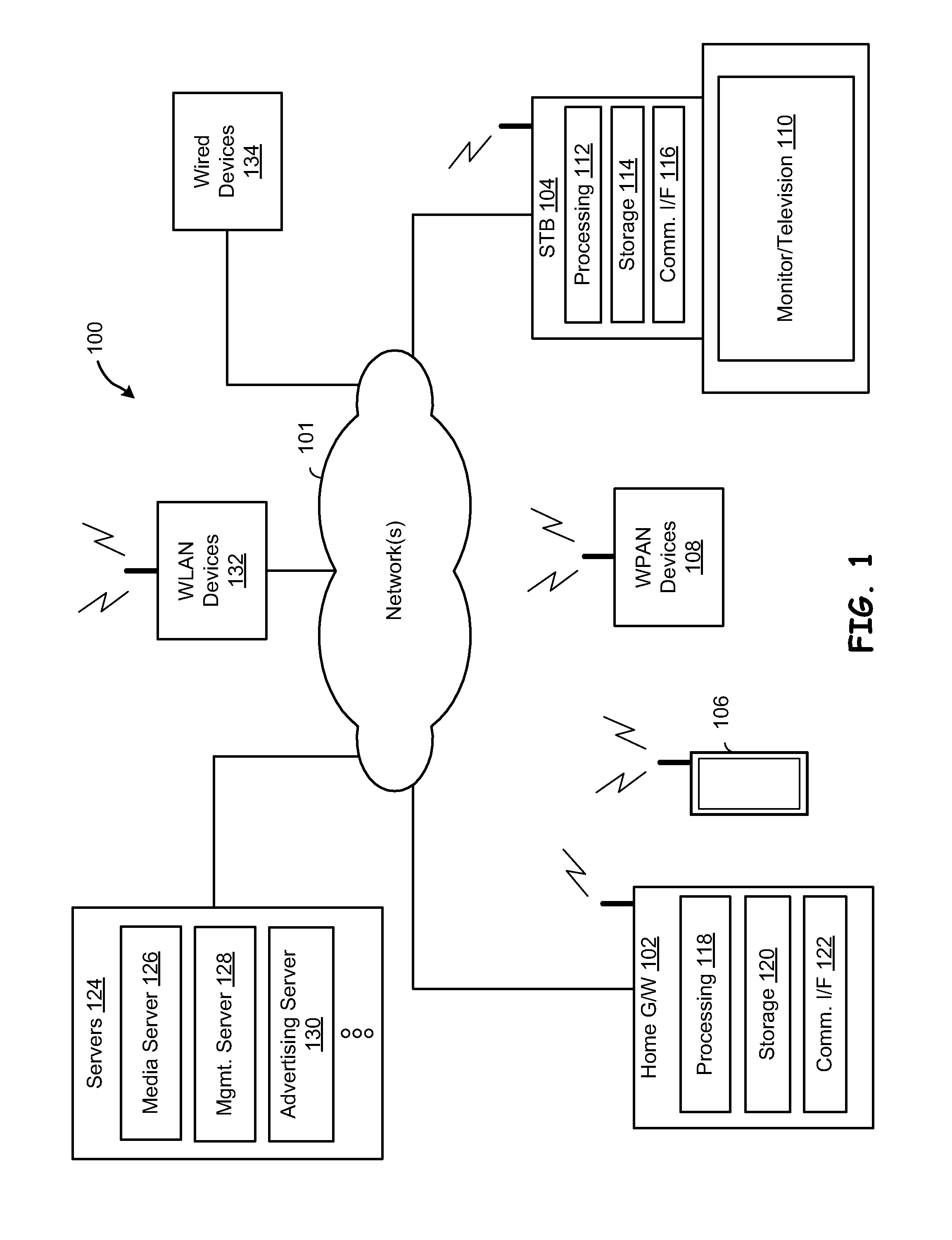
[0015]FIG. 1 is a system diagram illustrating components of a system 100 including circuitry according to one or more embodiments of the present disclosure. The illustrated system includes a home gateway (G / W) 102, a set top box (STB) 104, one or more communications network(s) 101, one or more smartphones and / or other mobile computing devices (e.g., tablet devices and laptop computers) 106, one or more wireless PAN (WPAN) devices 108, servers 124, one or more wireless LAN (WLAN) devices 132, and one or more wired devices 134.

[0016]In the illustrated system 100, each of the home G / W 102 and STB 104 includes processing 118 / 112, storage 120 / 114, and communication interface 122 / 116 resources. The STB 104 may service, for example, a coupled entertainment system, which may include a monitor / television 110 and sound system. Servers 124 may include, for example, a media server 126, a management server 128, an advertising server 132, etc., to support various local, distributed and / or cloud-b...


PUM


Abstract

Compensation circuitry includes a resistor and transistor coupled in series with a reference current source to generate a variable reference voltage that is provided, via a voltage regulator, to bias elements of a core circuit in order to establish an operating current in the core circuit. In one embodiment, the resistor and transistor of the compensation circuitry are of similar construction to the bias elements of the core circuit, such that fluctuations in the ratio of the reference current and the operating current of the core circuit are minimized over process, supply voltage and temperature variations. The voltage regulator may be a low dropout regulator. In various embodiments, the core circuit may comprise a resistor biased voltage controlled oscillator, a differential current mode logic (CML) input to single CMOS output circuit, or like circuitry that may be sensitive to phase noise or requires low power operation.

Description

CROSS REFERENCE TO RELATED PATENTS / PATENT APPLICATIONSProvisional Priority Claims[0001]The present U.S. Utility patent application claims priority pursuant to 35 U.S.C. §119(e) to the following U.S. Provisional patent application which is hereby incorporated herein by reference in its entirety and made part of the present U.S. Utility patent application for all purposes:[0002]1. U.S. Provisional Patent Application Ser. No. 61 / 807,692, entitled “LOW POWER BIAS COMPENSATION SCHEME UTILIZING A RESISTOR BIAS,” (Attorney Docket No. BP31812), filed Apr. 2, 2013, pending.BACKGROUND OF THE INVENTION[0003]1. Technical Field of the Invention[0004]The invention relates generally to bias compensation circuitry; and, more particularly, it relates to integrated compensation circuitry for reducing the effects of process, voltage and temperature variations.[0005]2. Description of Related Art[0006]In the design of electronic circuits, close attention must often be given to various sources of electri...

Claims


Application Information

Patent Timeline
Patent Type & Authority Applications(United States)
IPC IPC(8): H02M3/158
CPCH02M3/158H03B5/04H03B5/1212H03B5/1215H03B5/1228H03B5/1253
Inventor LEE, CHANG-HYEONKABALICAN, LINDEL DAVIDCHAMBERS, MARK JONATHAN
Owner AVAGO TECH WIRELESS IP SINGAPORE PTE
Why Eureka
Try Eureka