

Enhanced architectures of voltage-controlled oscillators with single inductor (VCO-1L)
a voltage-controlled oscillator and inductor technology, applied in the direction of oscillator generators, pulse automatic control, climate sustainability, etc., to achieve the effects of low phase noise, reduced power consumption, and high frequency stability
- Summary
- Abstract
- Description
- Claims
- Application Information
AI Technical Summary
Benefits of technology
Problems solved by technology
Method used
Image

Examples
Embodiment Construction
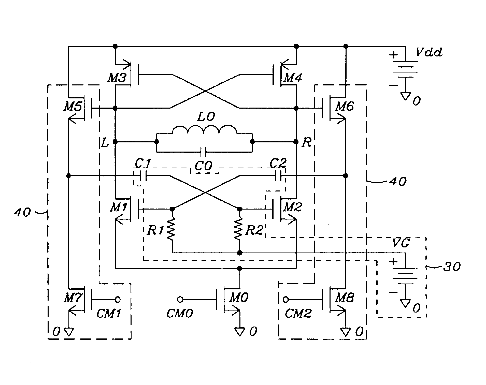
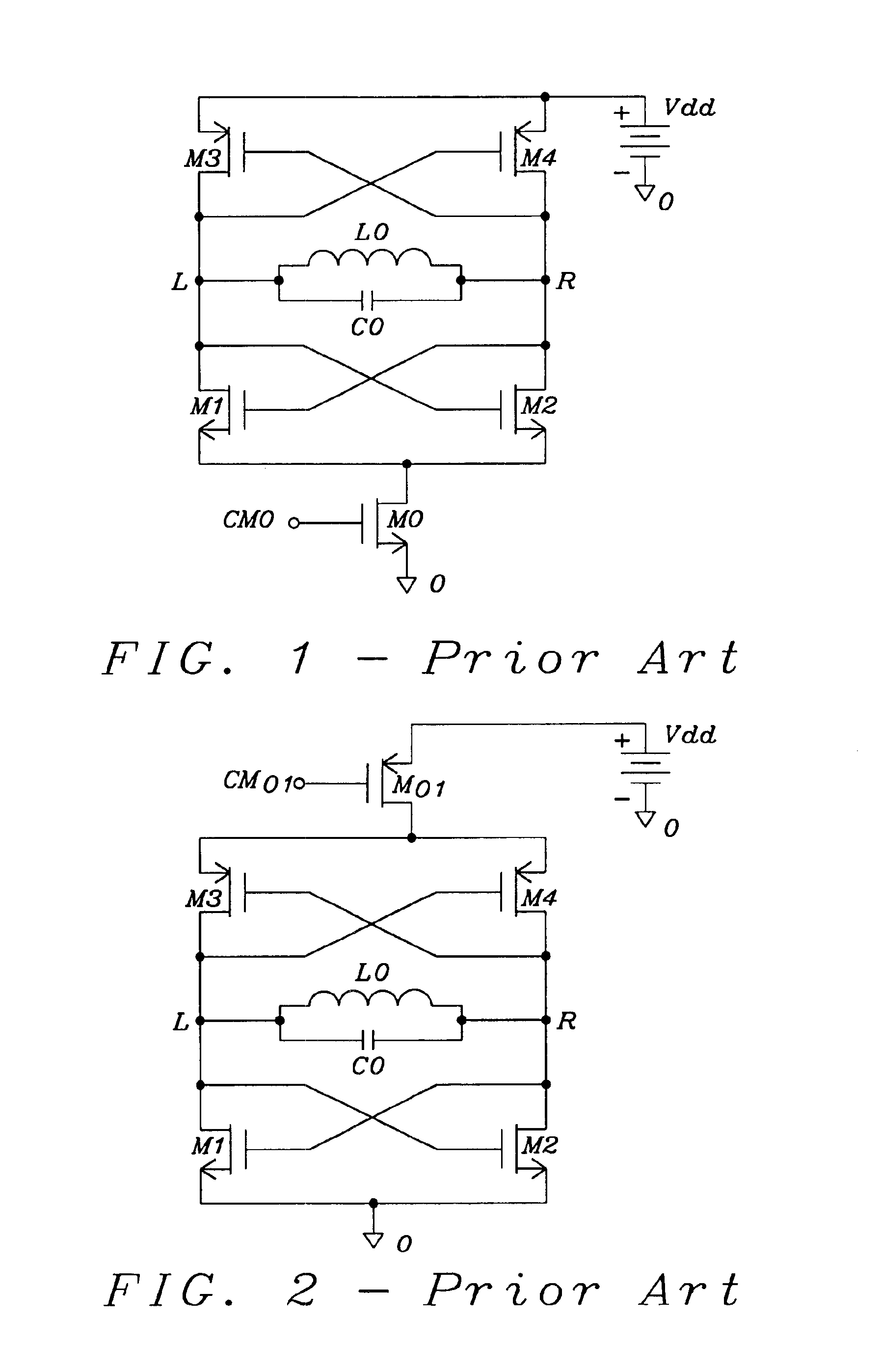
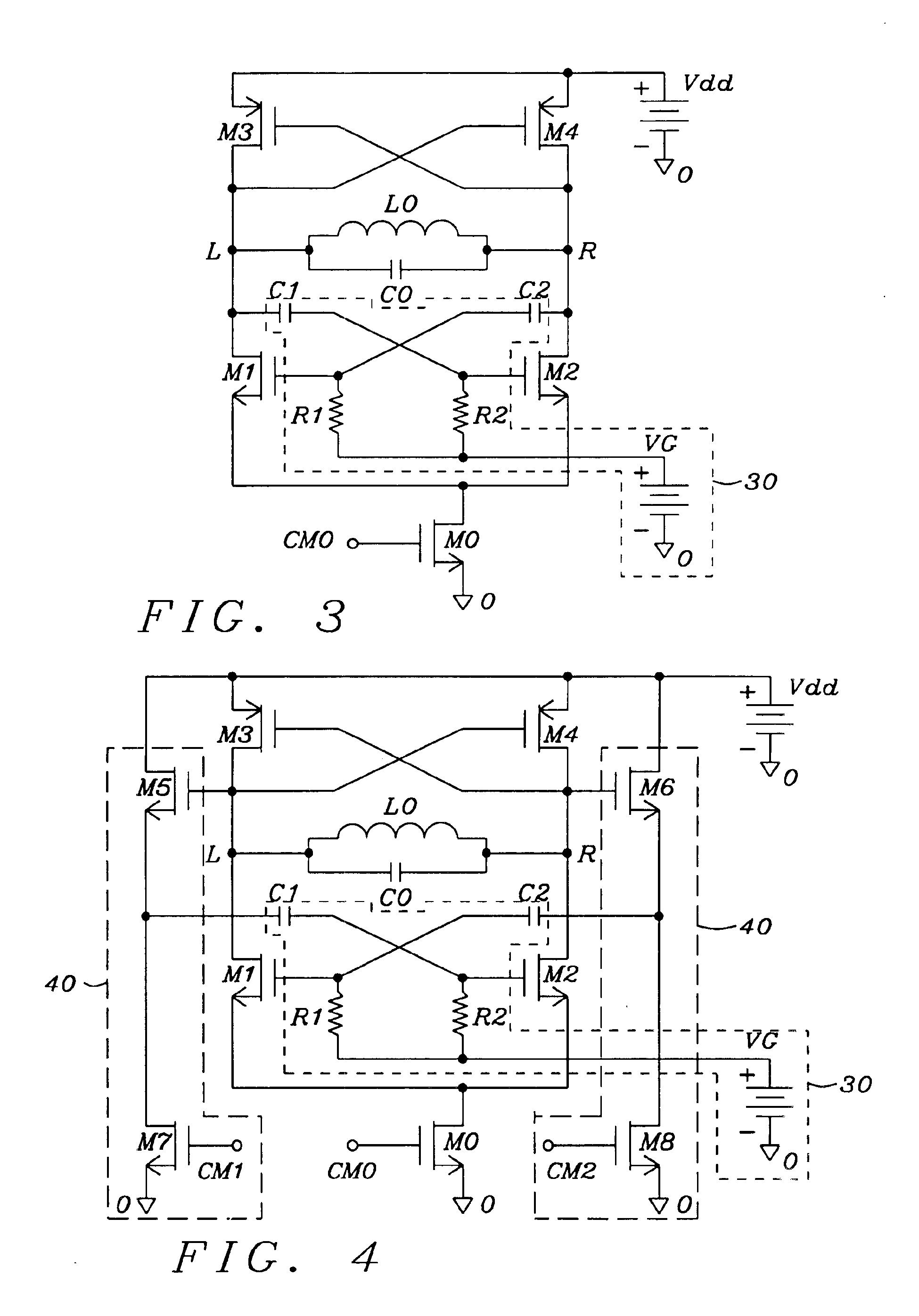
Disclosed are five different preferred embodiments of enhancements to prior art voltage controlled oscillators.
FIG. 3 shows a circuit according to the present invention based on the referred prior art circuit as shown in FIG. 1 prior art, characterized by means of an additional timing control 30. In the preferred embodiment shown in FIG. 3 said additional timing control is performed by capacitors C1 and C2, resistors R1 and R2 and a threshold voltage VG. The capacitors remove the DC connection gate-drain of the cross coupled transistors and provide thus the possibility to set time instances via the resistors when the transistors M1 and M2 will open and close. This depends of course from the threshold voltage typical for the specific transistor in use, denoted usually by Vth or in case of bipolar transistors, this is the Shockley voltage, usually in the range of 0.6 to 0.9 Volts.
The rest of the structure of the circuit is without changes compared to the circuit shown in FIG. 1 prior ...
PUM
 Abstract
Description
Claims
Application Information