Electronic device, quantum interference device, atomic oscillator, electronic apparatus, and moving object

a quantum interference and electronic technology, applied in the field of electronic devices, can solve the problems of reducing the distance between the two electronic components in the package, and achieve the effect of excellent reliability

Active Publication Date: 2014-10-02
MICROCHIP TECH INC
View PDF9 Cites 16 Cited by
  • Summary
  • Abstract
  • Description
  • Claims
  • Application Information

AI Technical Summary

Benefits of technology

[0034]The moving object h

Problems solved by technology

These problems are conspicuous when the distances between the package and the electronic components and the distance between the two electronic components in the package decrease according to a reduction in the size of the electronic

Method used


Image

  • Electronic device, quantum interference device, atomic oscillator, electronic apparatus, and moving object
  • Electronic device, quantum interference device, atomic oscillator, electronic apparatus, and moving object
  • Electronic device, quantum interference device, atomic oscillator, electronic apparatus, and moving object

Examples


Embodiment Construction

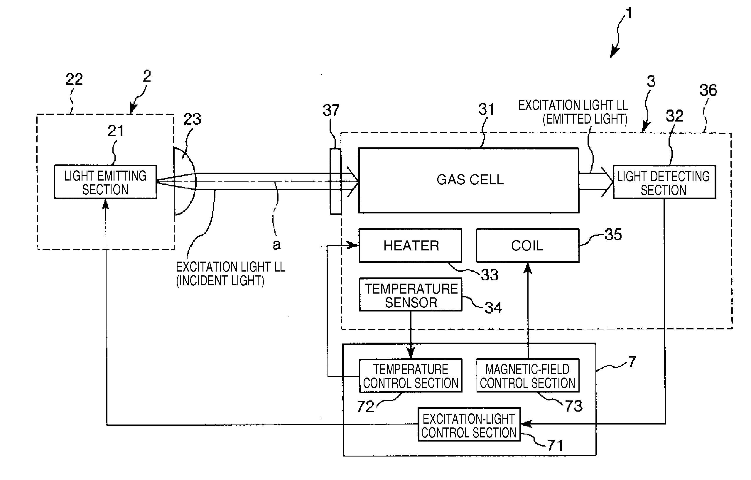
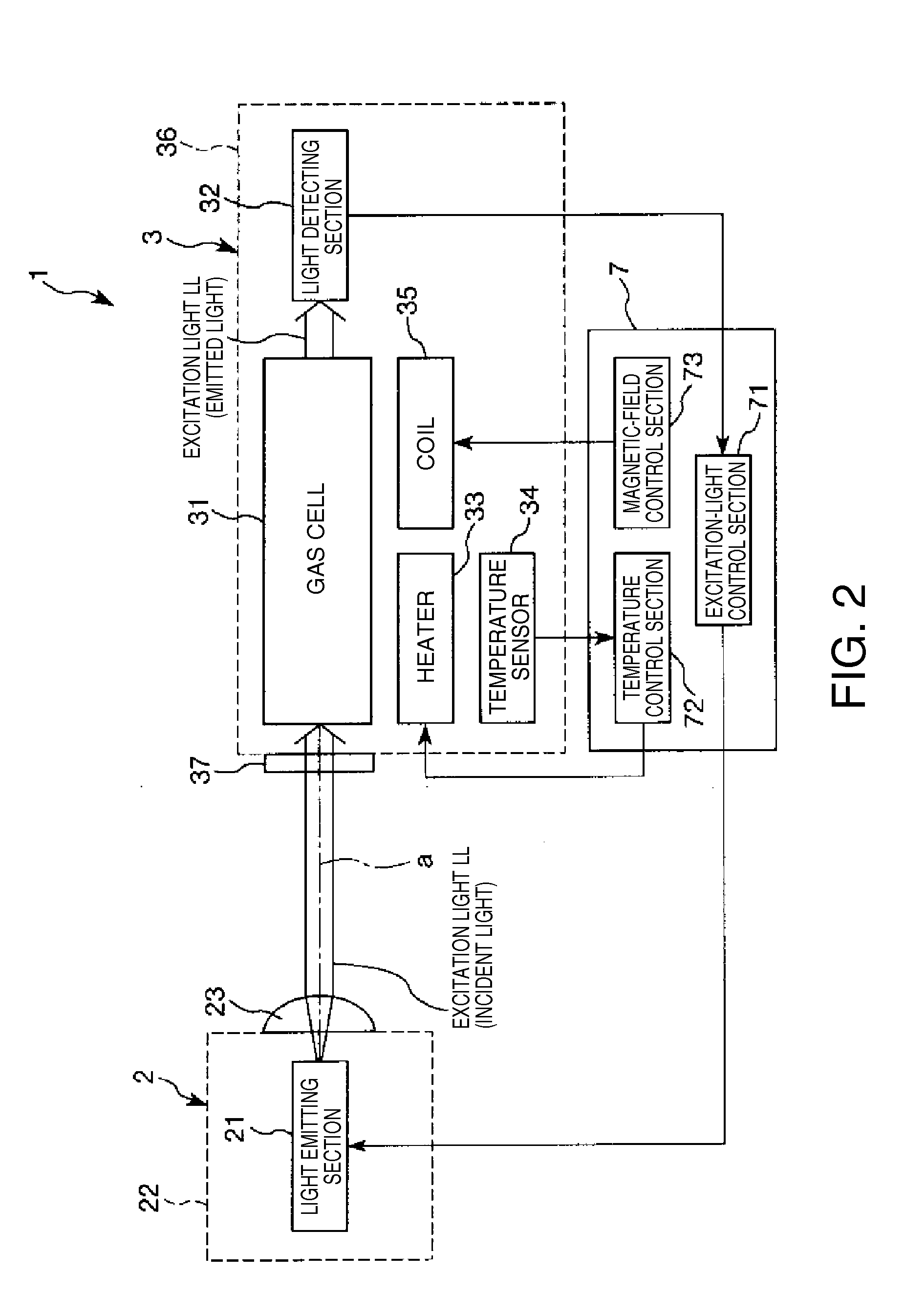
[0044]An electronic device, a quantum interference device, an atomic oscillator, an electronic apparatus, and a moving object according to the invention are explained in detail below with reference to an embodiment shown in the accompanying drawings.

1. Atomic Oscillator (Quantum Interference Device)

[0045]First, the atomic oscillator according to the invention (the atomic oscillator including the quantum interference device according to the invention) is explained. In the following explanation, an example in which the quantum interference device according to the invention is applied to the atomic oscillator is explained. However, the quantum interference device according to the invention is not limited to this. The quantum interference device according to the invention can also be applied to, for example, a magnetic sensor and a quantum memory besides the atomic oscillator.

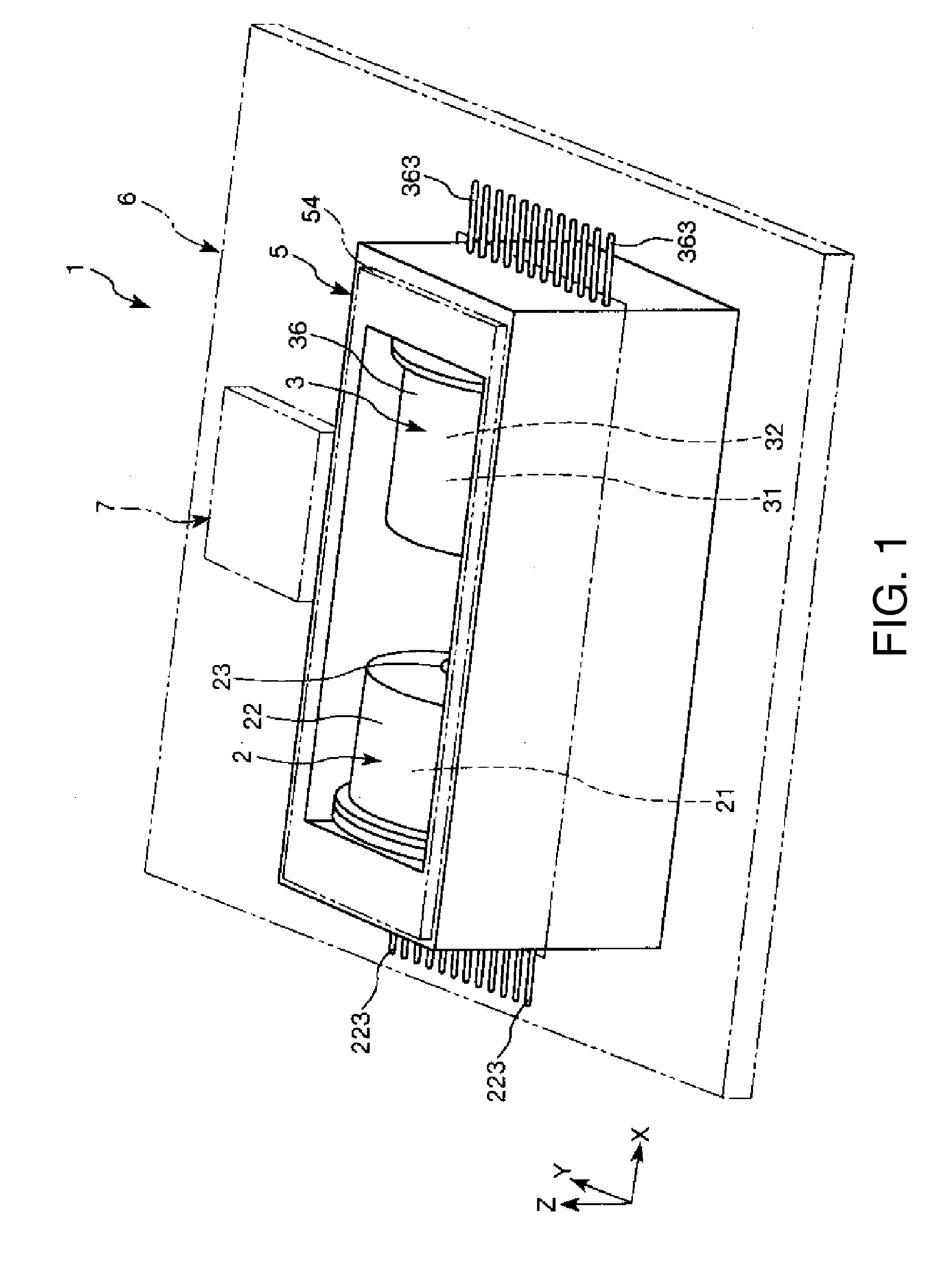
[0046]FIG. 1 is a perspective view showing an atomic oscillator according to an embodiment of the invention. FIG...


PUM


Abstract

An atomic oscillator includes a first unit and a second unit arranged to be separated from each other and a package including an internal space in which the first unit and the second unit are housed in a state in which the internal space is decompressed to pressure lower than the atmospheric pressure. The reflectance of the outer surfaces of the first unit and the second unit to an electromagnetic wave having a wavelength of 4 μm is equal to or higher than 50%.

Description

BACKGROUND[0001]1. Technical Field[0002]The present invention relates to an electronic device, a quantum interference device, an atomic oscillator, an electronic apparatus, and a moving object.[0003]2. Related Art[0004]In an electronic device in which an electronic component subjected to temperature control is housed in a package, it is generally performed to evacuate the package for the purpose of preventing heat conduction from the outside of the package to the electronic component in the package.[0005]For example, an electronic device disclosed in JP-UM-A-57-155810 (Patent Literature 1), a container (an electronic component) on the inner side, in which a crystal oscillation circuit, a heat generating element, and a thermosensitive element are housed, is housed in another container (a package) on the outer side and a space between the containers is evacuated.[0006]However, in the electronic device disclosed in Patent Literature 1, although heat conduction and transfer of heat by c...

Claims


Application Information

Patent Timeline
IPC IPC(8): H01S1/06
CPCH01S1/06H01S5/0687G04F5/145H01S5/02H01S5/02212H01S5/02446H01S5/183H03B17/00H03L1/04H03L7/26
Inventor CHINDO, KOJI
Owner MICROCHIP TECH INC
Why Eureka
Try Eureka