Method of manufacturing semiconductor chips

a semiconductor chip and manufacturing method technology, applied in semiconductor devices, electrical equipment, electric discharge tubes, etc., can solve the problems of reducing limiting the improvement of the chip yield per, and chipping on the corner parts (edges), so as to improve the chip yield and reduce the chipping. , the effect of improving the handling ability

Active Publication Date: 2014-10-02
PANASONIC INTELLECTUAL PROPERTY MANAGEMENT CO LTD
View PDF4 Cites 10 Cited by
  • Summary
  • Abstract
  • Description
  • Claims
  • Application Information

AI Technical Summary

Benefits of technology

[0019]According to the method of manufacturing semiconductor chips in accordance with the invention, var...

Problems solved by technology

The DBG technique with use of the dicer, however, has following problems.
Firstly, a constraint of thickness of the blade (at least on the order of 40 to 50 μm) imposes limitations on improvement in chip yield per semiconductor wafer.
Further, because the semiconductor wafer attached on the thin protection tape is diced int...

Method used


Image

  • Method of manufacturing semiconductor chips
  • Method of manufacturing semiconductor chips
  • Method of manufacturing semiconductor chips

Examples


Embodiment Construction

[0027]An embodiment of the invention will be described below in detail with reference to the accompanying drawings.

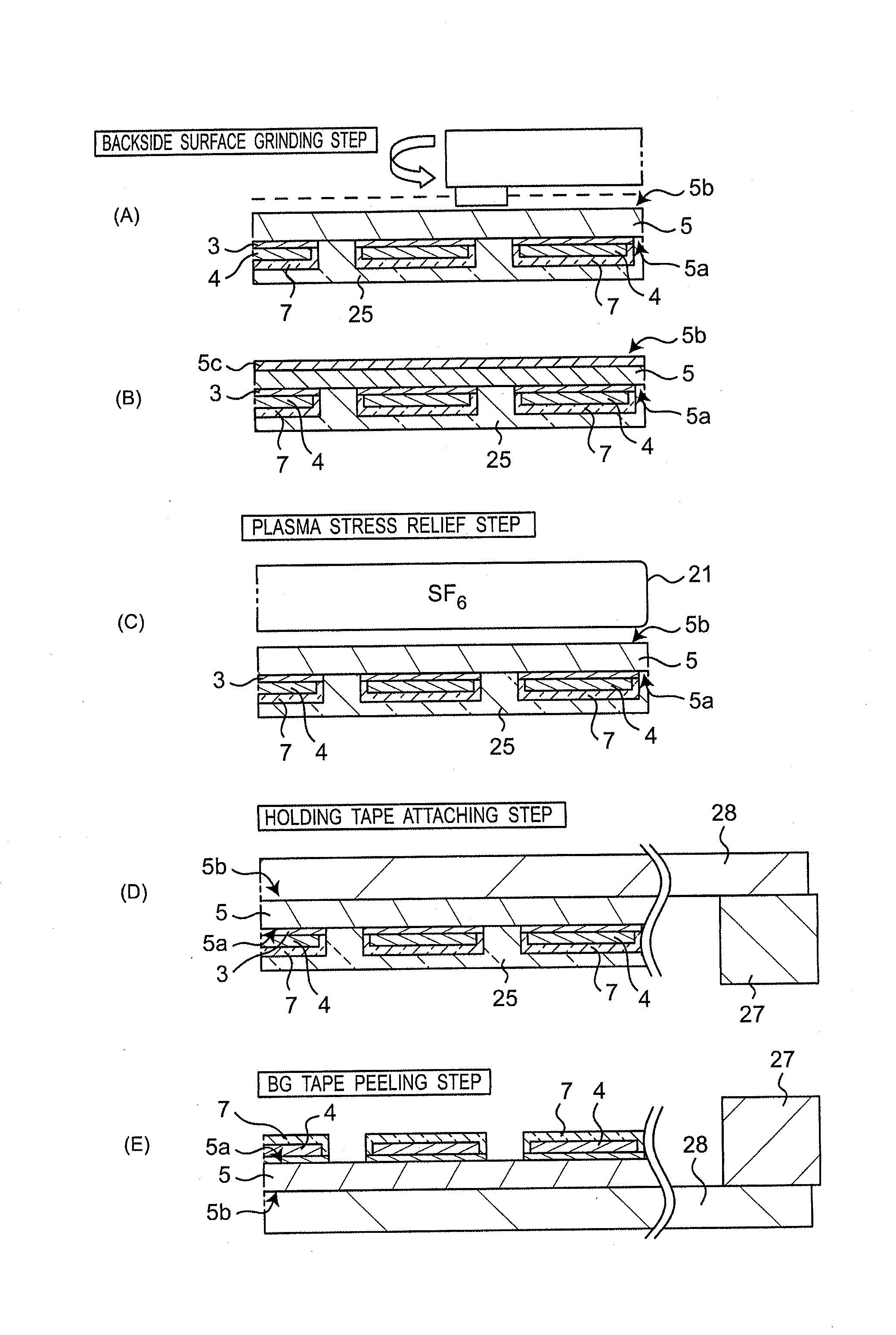
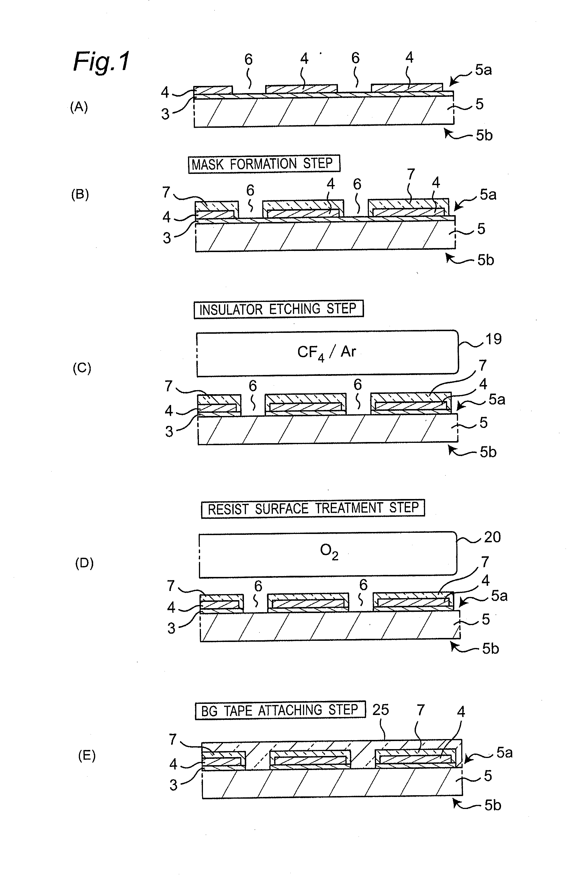
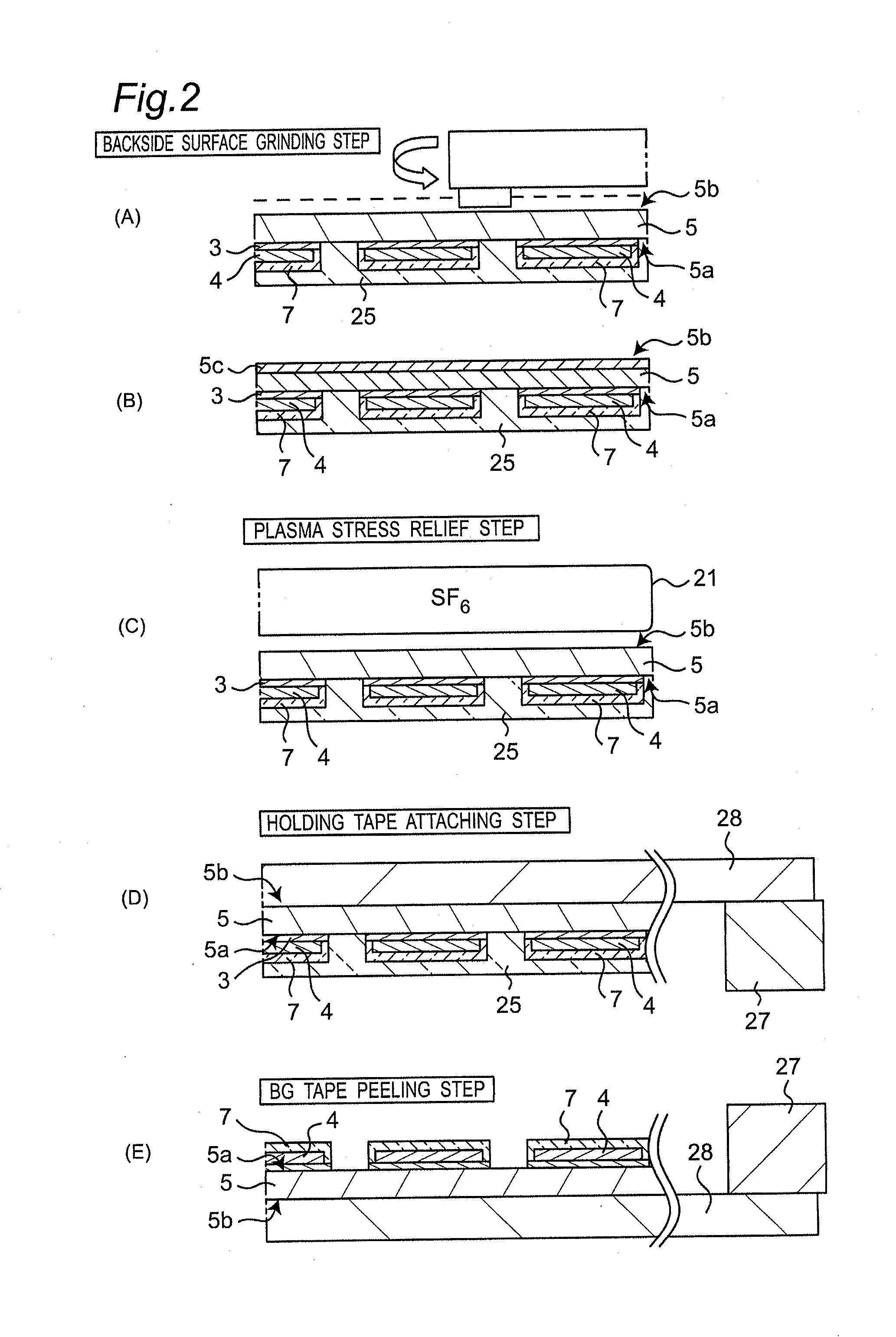
[0028]FIGS. 1 through 3 are schematic sections showing a method of manufacturing semiconductor chips in accordance with an embodiment of the invention. FIG. 4 shows a semiconductor chip 1 manufactured by the manufacturing method. The semiconductor chip 1 has a die 2, an insulating film 3 formed on the die 2, and an IC section (semiconductor element section) 4 formed on the insulating film 3. In the embodiment, the die 2 is made of Si or Si-based material and the insulating film 3 is made of SiO2. Materials of the die 2 and the insulating film 3, however, are not limited thereto. For instance, the insulating film 3 may be made of SiN, SiOC, Low-k or the like.

[0029]As shown in FIG. 1(A), the insulating film 3 is formed on a front surface (first surface) 5a of the semiconductor wafer 5, and a plurality of IC sections 4 are formed thereon. There are gaps (dividing region 6)...


PUM


Abstract

Provided is a method of manufacturing semiconductor chips superior in chip yield, reduction in chipping, and handling ability. An insulating film in a dividing region is removed by plasma etching to a front surface. Then, roughness on a resist mask formed on the front surface is removed by plasma treatment before a BG tape is attached. After a semiconductor wafer is thinned by grinding of a backside surface thereof, the BG tape is peeled. The semiconductor wafer is divided into individual semiconductor chips by plasma etching from the front surface thereof.

Description

TECHNICAL FIELD[0001]The present invention relates to a method of manufacturing semiconductor chips in which a semiconductor wafer is divided and diced into individual pieces.BACKGROUND ART[0002]In a known method of manufacturing semiconductor chips by dividing and dicing a semiconductor wafer into individual pieces, the semiconductor wafer is mechanically divided by a blade of a dicer. For instance, mechanical dicing with use of DBG (Dicing Before Grinding) technique is disclosed in Patent Literature 1. In the DBG technique disclosed in Patent Literature 1, grooves are formed on an element formation surface (front surface) of a semiconductor wafer by a blade, followed by attachment of a protection tape on the front surface. Subsequently, a surface (backside surface) of the semiconductor wafer opposed to the front surface is ground until the grooves are exposed, so that the wafer is diced into individual semiconductor chips.[0003]The DBG technique with use of the dicer, however, has...

Claims


Application Information

Patent Timeline
IPC IPC(8): H01L21/78H01L21/683H01L21/304
CPCH01L21/78H01L21/0273H01L21/304H01L21/3065H01J37/321H01L21/31138H01L21/6836H01L2221/68327H01L2221/6834H01L21/31116H01L2221/68386
Inventor HARIKAI, ATSUSHI
Owner PANASONIC INTELLECTUAL PROPERTY MANAGEMENT CO LTD
Why Eureka
Try Eureka