Multilayer ceramic substrate and electronic component using same
- Summary
- Abstract
- Description
- Claims
- Application Information
AI Technical Summary
Benefits of technology
Problems solved by technology
Method used
Image

Examples
Embodiment Construction
[0050]Features of the present invention will be described in more detail with reference to embodiments of the present invention below.
[0051][Configuration of Multilayer Ceramic Substrate]
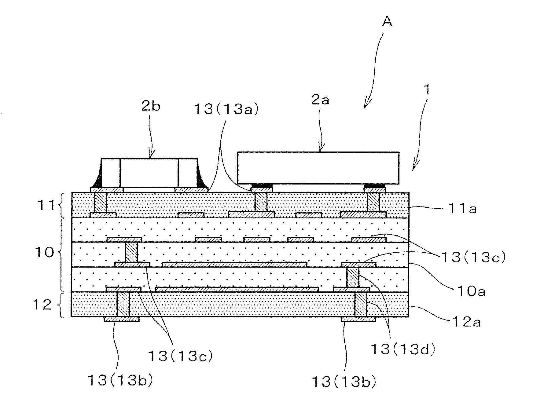
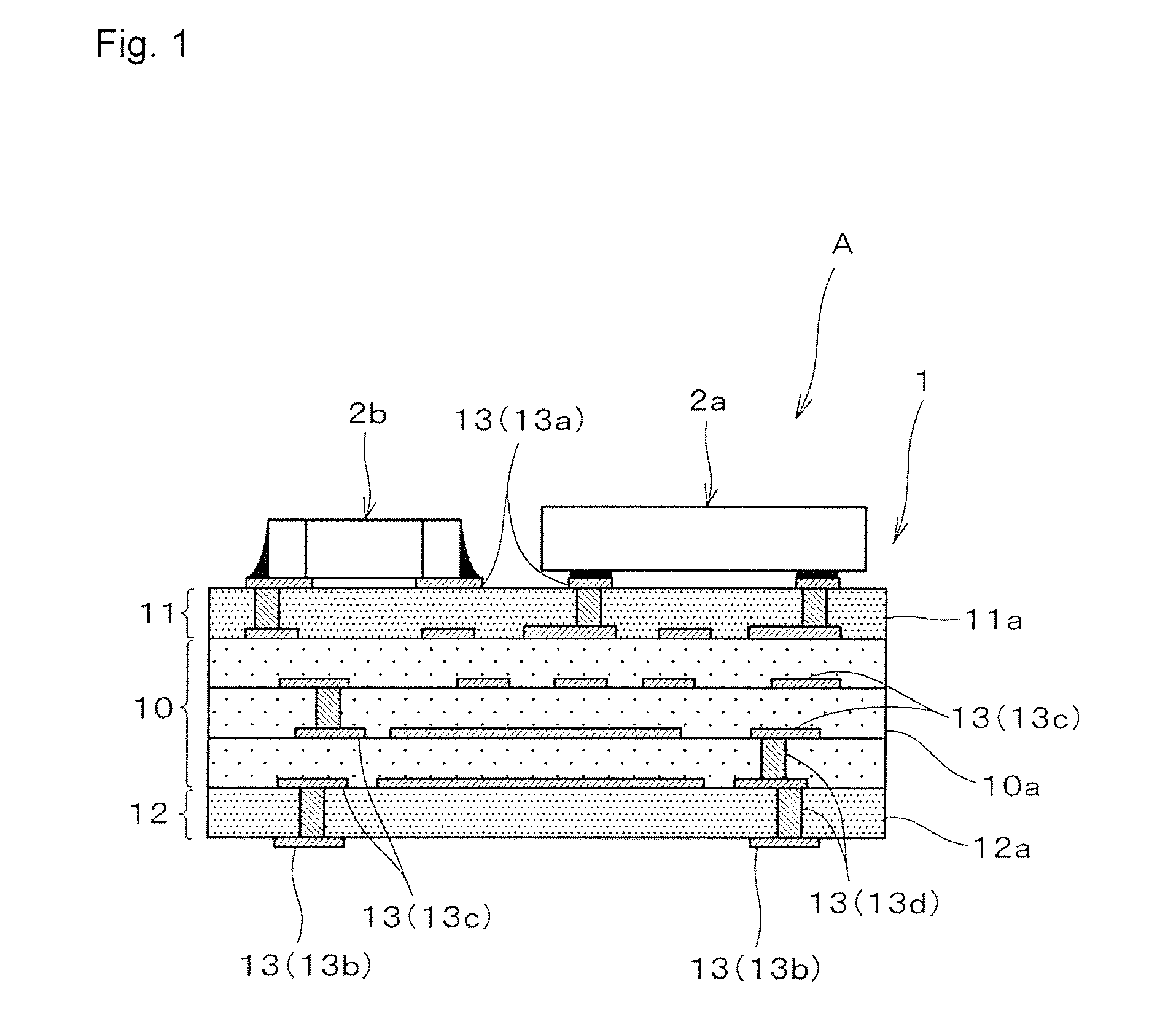
[0052]FIG. 1 is a front cross-sectional view illustrating an electronic component according to an embodiment of the present invention, where chip components are mounted on surface electrodes of a multilayer ceramic substrate according to an embodiment of the present invention.
[0053]The multilayer ceramic substrate 1 constituting the electronic component A has a stacked structure including an inner-layer section 10 and first and second surface-layer sections 11, 12 stacked and provided on both principal surfaces of the inner-layer section 10 so as to sandwich the inner-layer section 10 in a stacking direction.
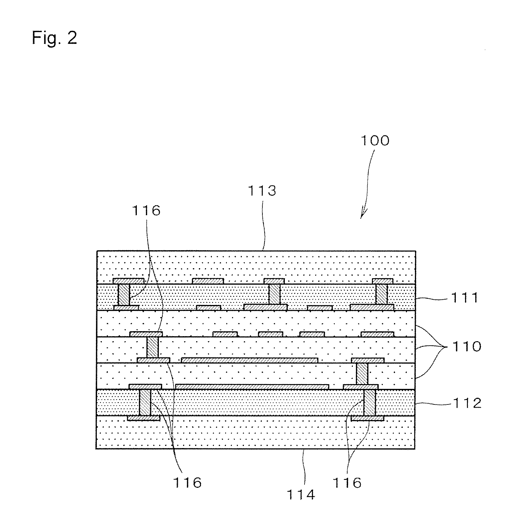
[0054]It is to be noted that the inner-layer section 10 includes at least one inner-layer section ceramic layer 10a, whereas the first and second surface-layer sections 11, 12 also respectively ...
PUM
 Abstract
Description
Claims
Application Information