Display device and method of manufacturing display device

Active Publication Date: 2014-10-16
PANASONIC LIQUID CRYSTAL DISPLAY CO LTD
View PDF3 Cites 6 Cited by
  • Summary
  • Abstract
  • Description
  • Claims
  • Application Information

AI Technical Summary

Benefits of technology

[0004]Here, the organic protective film is formed of, for example, photosensitive resist material, and is formed to be thicker than other insulting films. The organic protective film is generally opened by development processing in an exposure step, and it is formed to be thicker

Problems solved by technology

Thus, it is impossible to open the organic pr

Method used


Image

  • Display device and method of manufacturing display device
  • Display device and method of manufacturing display device
  • Display device and method of manufacturing display device

Examples


first embodiment

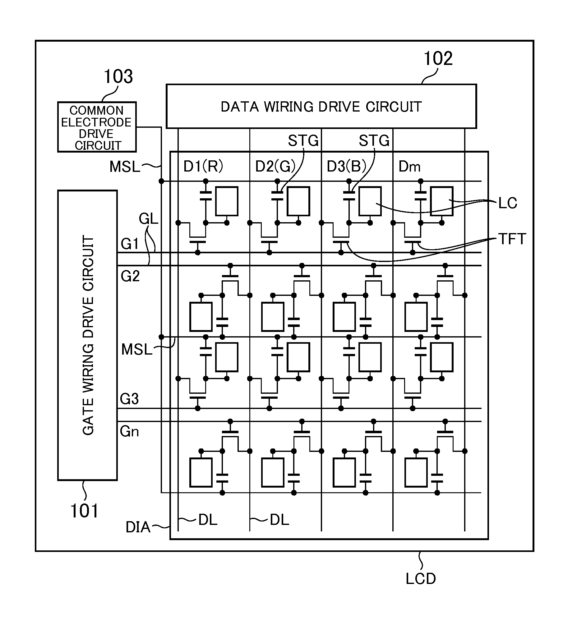
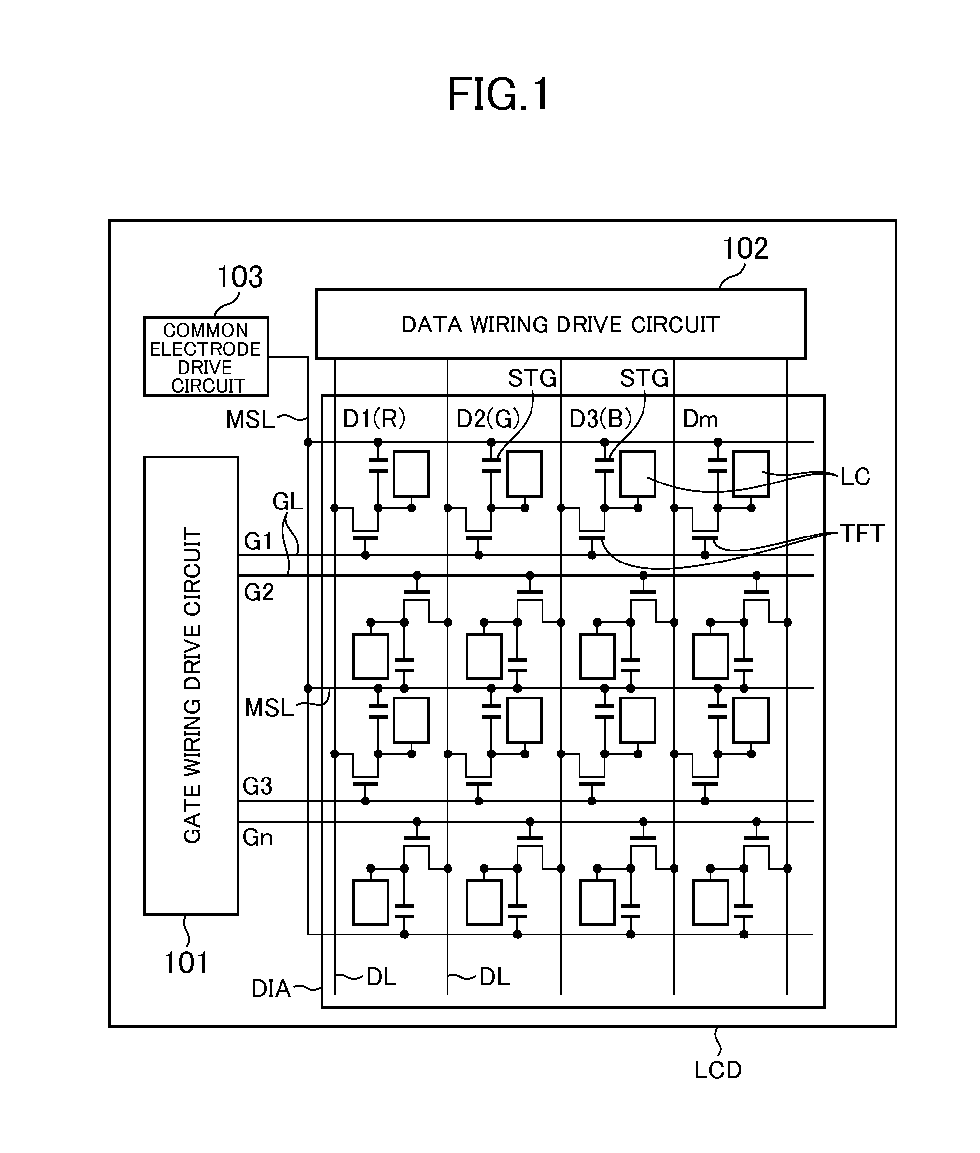
[0057]FIG. 1 is a diagram schematically illustrating a display device according to a first embodiment of the present application. As shown in FIG. 1, the display device LCD includes a gate wiring drive circuit 101, a data wiring drive circuit 102, a common electrode drive circuit 103 and a pixel region DIA.

[0058]A gate voltage is supplied from the gate wiring drive circuit 101 through gate wirings G1, G2, . . . and Gn and a video data voltage is supplied from the data wiring drive circuit 102 through data wirings D1, D2, . . . and Dm to the pixel region DIA as an active matrix display. Then, a thin film transistor TFT is turned on and off to feed a data voltage to a pixel electrode. Then, by an electric field between a common voltage supplied from the common electrode drive circuit 103 and the data voltage, a liquid crystal layer LC is driven.

[0059]In order to prevent a voltage drop in the liquid crystal layer LC, a retention capacity STG is formed in each pixel region. The supply o...

second embodiment

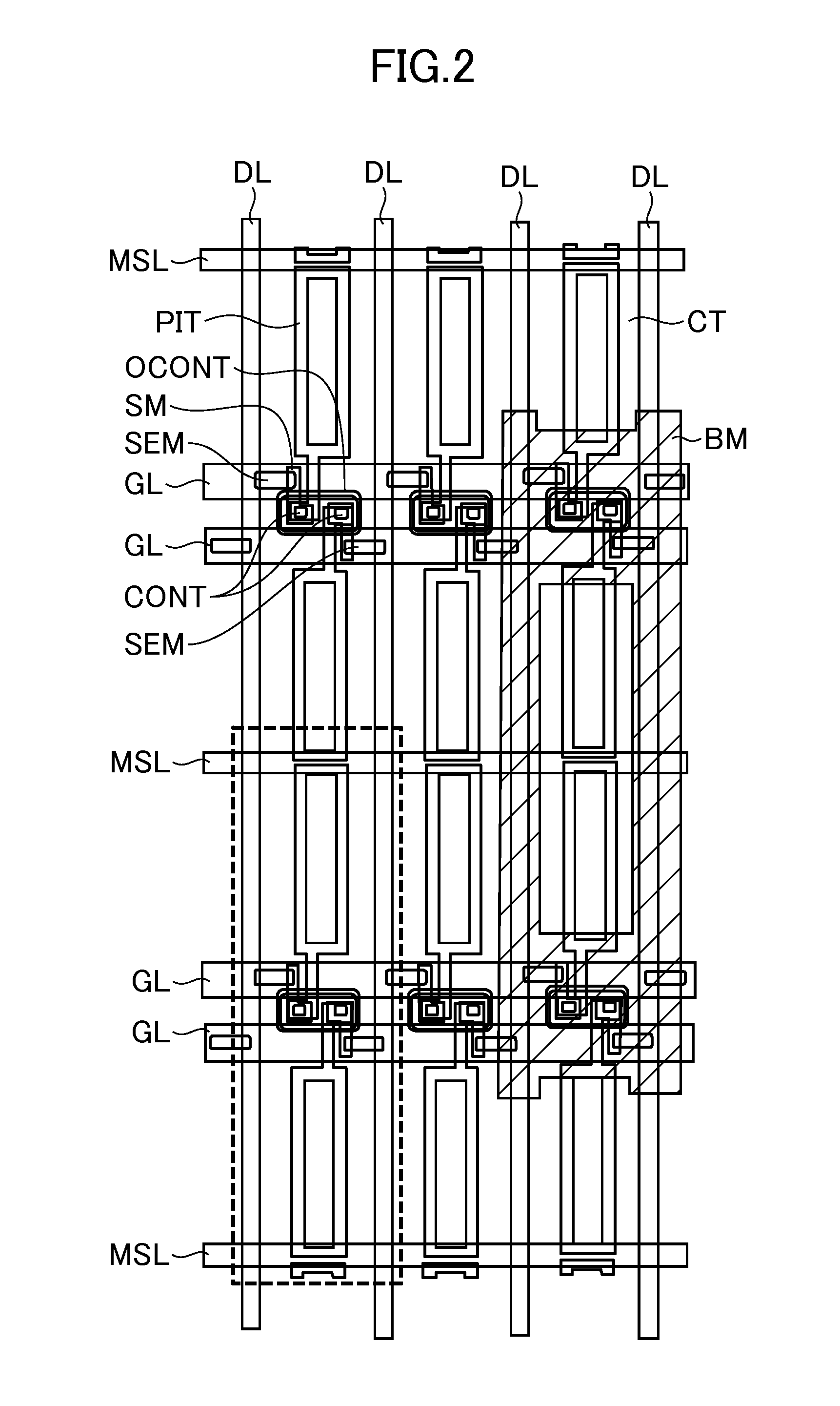
[0119]FIG. 14 is a diagram for illustrating a display device according to a second embodiment of the present application. As shown in FIG. 14, as in the first embodiment described above, the display device LCD includes the gate wiring drive circuit 101, the data wiring drive circuit 102, the common electrode drive circuit 103 and the pixel region DIA. The present embodiment mainly differs from the first embodiment in that the gate wirings are not arranged adjacently every two gate wirings, and that the common electrode wiring MSL is not shared.

[0120]As in the first embodiment, a scanning voltage is supplied from scanning (gate) wirings G1, G2, . . . and Gn and a video data voltage is supplied from data wirings D1, D2, . . . and Dn to the pixel region DIA. Then, the thin film transistor TFT is turned on and off to feed the data voltage to the liquid crystal layer LC, and an electric field between this and the common voltage drives the liquid crystal layer LC. In order to prevent a vo...


PUM


Abstract

A display device includes a plurality of pixels arranged in a matrix. Each of the plurality of pixels includes a transistor and a pixel electrode arranged above the transistor through a first protective film and a second protective film. Among the plurality of pixels, the pixel electrodes of two pixels adjacent in a column direction are connected to corresponding source electrodes of the two pixels through second and third contact holes respectively. The second and third contact holes are formed in the first protective film within a first contact hole that is formed in the second protective film.

Description

CROSS-REFERENCE TO RELATED APPLICATION[0001]The present application claims priority from Japanese Application JP2013-084676 filed on Apr. 15, 2013, the content of which is hereby incorporated by reference into this application.TECHNICAL FIELD[0002]The present invention relates to a display device and a method of manufacturing a display device.BACKGROUND[0003]For example, as shown in the Japanese Patent Application Publication No. H09-230380, a display device is known that includes an organic protective film which is formed to cover a TFT, a gate wiring and a source wiring and a pixel electrode which is formed on the organic protective film. In the display device described above, a contact hole is provided in the organic protective film, and a source electrode and the pixel electrode of the TFT are electrically connected through the contact hole.SUMMARY[0004]Here, the organic protective film is formed of, for example, photosensitive resist material, and is formed to be thicker than o...

Claims


Application Information

Patent Timeline
IPC IPC(8): H01L27/12
CPCH01L27/124H01L27/127H01L27/1262H01L27/1248G02F1/133345G02F1/134336G02F1/136227G02F1/136286G02F1/1368
Inventor ONO, KIKUO
Owner PANASONIC LIQUID CRYSTAL DISPLAY CO LTD
Why Eureka
Try Eureka