Organic light emitting diode display device and method of fabricating the same

a light-emitting diode and display device technology, applied in the direction of thermoelectric device junction materials, semiconductor devices, electrical apparatus, etc., can solve the problems of non-uniform brightness, loss of lead lead in display devices by flat-panel displays

Active Publication Date: 2014-10-23
LG DISPLAY CO LTD
View PDF6 Cites 98 Cited by
  • Summary
  • Abstract
  • Description
  • Claims
  • Application Information

AI Technical Summary

Benefits of technology

[0011]Accordingly, the present invention is directed to an organic light emitting diode display and a method of fabrica...

Problems solved by technology

Although a cathode ray tube (CRT) has led the display device industry for several decades, the CRT has lost the lead in display devices by a flat panel display (...

Method used


Image

  • Organic light emitting diode display device and method of fabricating the same
  • Organic light emitting diode display device and method of fabricating the same
  • Organic light emitting diode display device and method of fabricating the same

Examples


Embodiment Construction

[0017]Reference will now be made in detail to the preferred embodiments, examples of which are illustrated in the accompanying drawings.

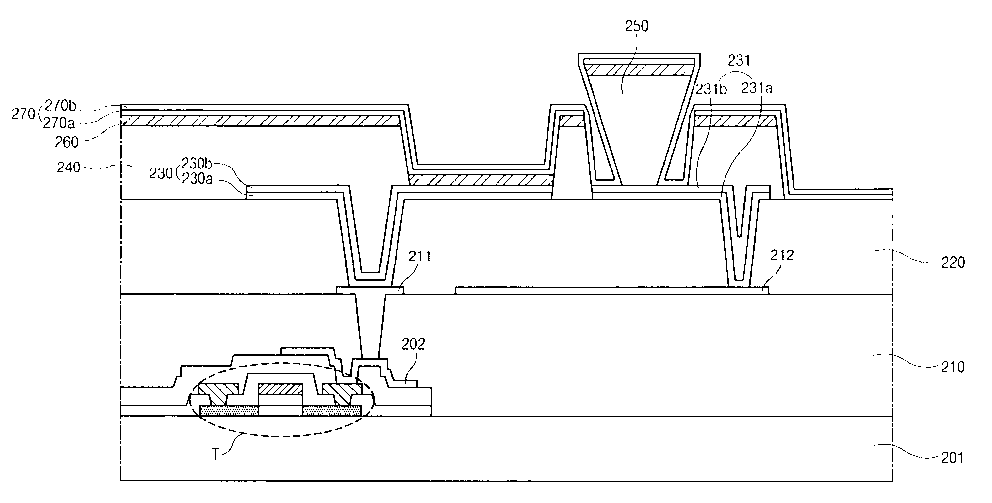
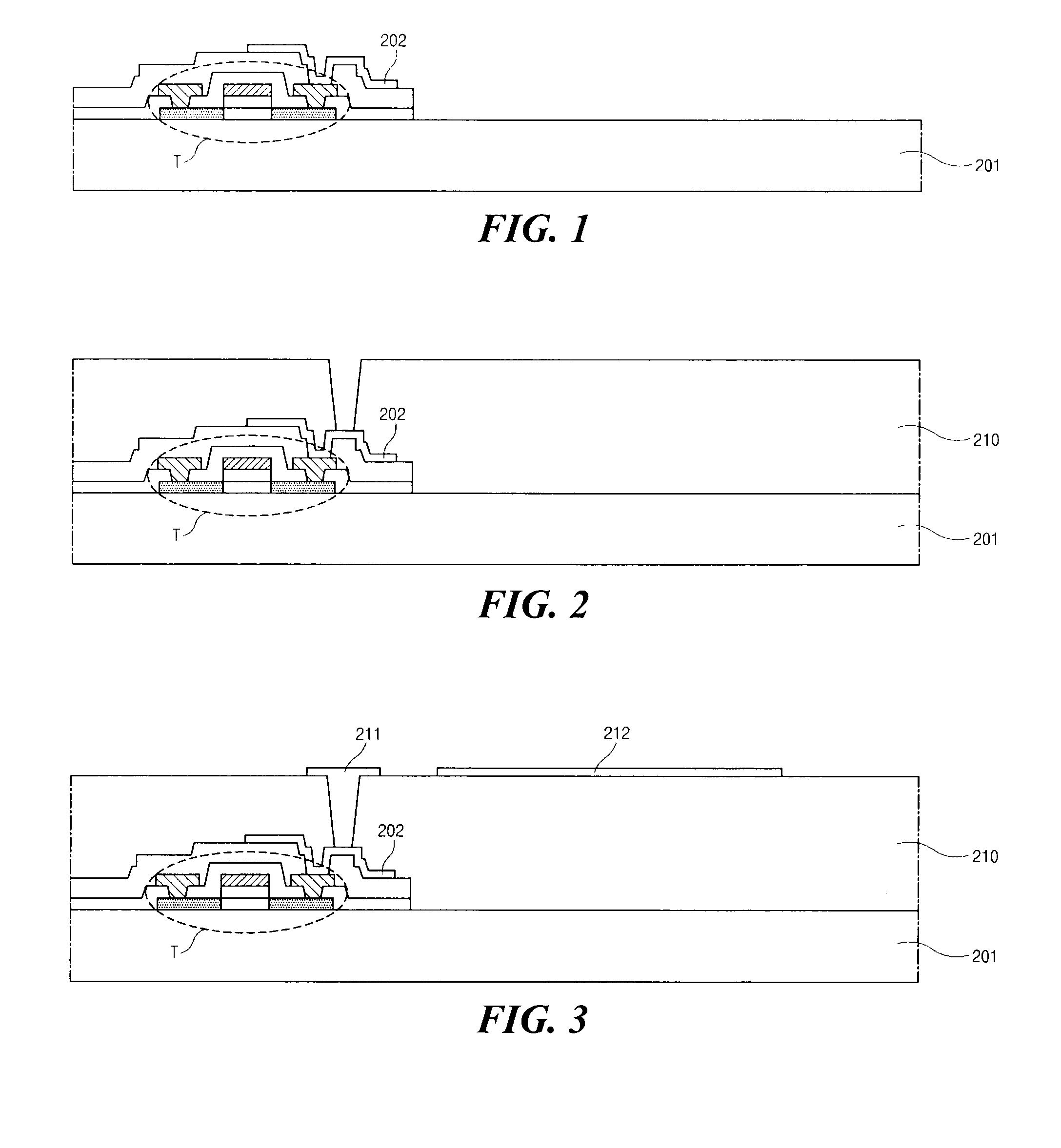
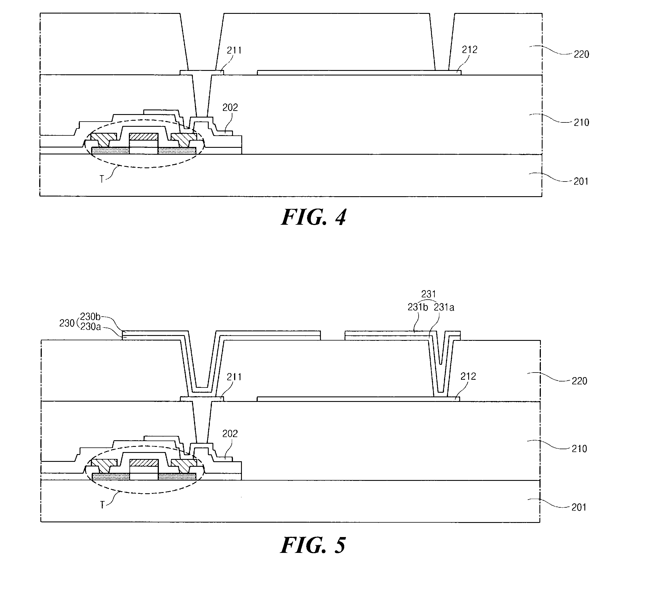
[0018]FIGS. 1 to 8 are cross-sectional views showing a method of fabricating an organic light emitting diode display device according to an embodiment of the present invention.

[0019]In FIGS. 1 to 8, an organic light emitting diode (OLED) display device according to an embodiment of the present invention includes a substrate 201, a thin film transistor (TFT) T, a first insulating layer 210, a connecting electrode 211, a first auxiliary electrode 212, a second insulating layer 220, an anode 230, a second auxiliary electrode 231, a bank layer 240, a separator 250, an organic emitting layer 260 and a cathode 270.

[0020]The substrate 201 may include one of a glass, a metal and a flexible material. The flexible material may include a plastic and a material having excellent thermal resistance and durability may be used as the flexible material. For example,...


PUM


Abstract

An organic light emitting diode display device, comprises: a thin film transistor on a substrate; a first insulating layer on the thin film transistor; a connecting electrode connected to the thin film transistor and a first auxiliary electrode on the first insulating layer; a second insulating layer on the connecting electrode and the first auxiliary electrode; an anode connected to the connecting electrode and a second auxiliary electrode spaced apart from the anode and connected to the first auxiliary electrode on the second insulating layer; a bank layer having a first contact hole exposing the anode and a second contact hole exposing the second auxiliary electrode on the anode and the second auxiliary electrode; an organic emitting layer on the anode in the first contact hole; and a cathode electrically connected to the second auxiliary electrode on the organic emitting layer.

Description

CROSS-REFERENCE TO RELATED APPLICATIONS[0001]The present application claims the benefit of priority of Korean Patent Application No. 10-2013-0044924 filed on Apr. 23, 2013, which is hereby incorporated by reference for all purposes as if fully set forth herein.BACKGROUND OF THE INVENTION[0002]1. Field of the Invention[0003]The present disclosure relates to an organic light emitting diode display device. The present disclosure also relates to an active matrix organic light emitting diode display device and a method of fabricating the same.[0004]2. Discussion of the Related Art[0005]Although a cathode ray tube (CRT) has led the display device industry for several decades, the CRT has lost the lead in display devices by a flat panel display (FPD) due to a large volume and a heavy weight. In the display market, up to recently, the FPD has gained in popularity due to a light weight and a thin profile as compared with the CRT having a high resolution.[0006]The FPD may include a liquid cry...

Claims


Application Information

Patent Timeline
IPC IPC(8): H01L27/32
CPCH01L27/3258H10K59/122H10K59/123H10K59/1315H10K50/824H10K50/8428H10K59/1201H10K59/32H10K50/81H10K50/814H10K50/82
Inventor PARK, SUNG-HEEKIM, BINN
Owner LG DISPLAY CO LTD
Why Eureka
Try Eureka