Single transistor random access memory using ion storage in two-dimensional crystals

a two-dimensional crystal and random access technology, applied in the field of universal memory, can solve the problems of low write speed and write/erase degradation, flash memory has its limitations, and the reliability of the definition of the on and off state is less reliabl

Active Publication Date: 2014-10-30
UNIV OF NOTRE DAME DU LAC
View PDF1 Cites 40 Cited by
  • Summary
  • Abstract
  • Description
  • Claims
  • Application Information

AI Technical Summary

Problems solved by technology

Flash memory has its limitations, however, such as relatively low write speed and write/erase degradation.
While RRAM appears to be a promising nonvolatile memory, there are a number of challenges associated with RRAM.
One illustrative challenge is that the distribution cell resistances obtained after writing an RRAM memory array a...

Method used


Image

  • Single transistor random access memory using ion storage in two-dimensional crystals
  • Single transistor random access memory using ion storage in two-dimensional crystals
  • Single transistor random access memory using ion storage in two-dimensional crystals

Examples


Embodiment Construction

[0011]The following description of example apparatus and methods is not intended to limit the scope of the disclosure to the precise form or forms detailed herein. Instead the following description is intended to be illustrative so that others may follow its teachings.

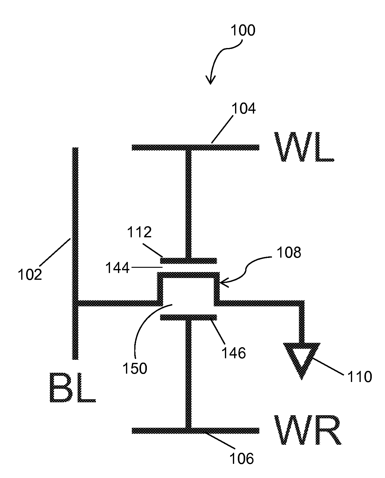
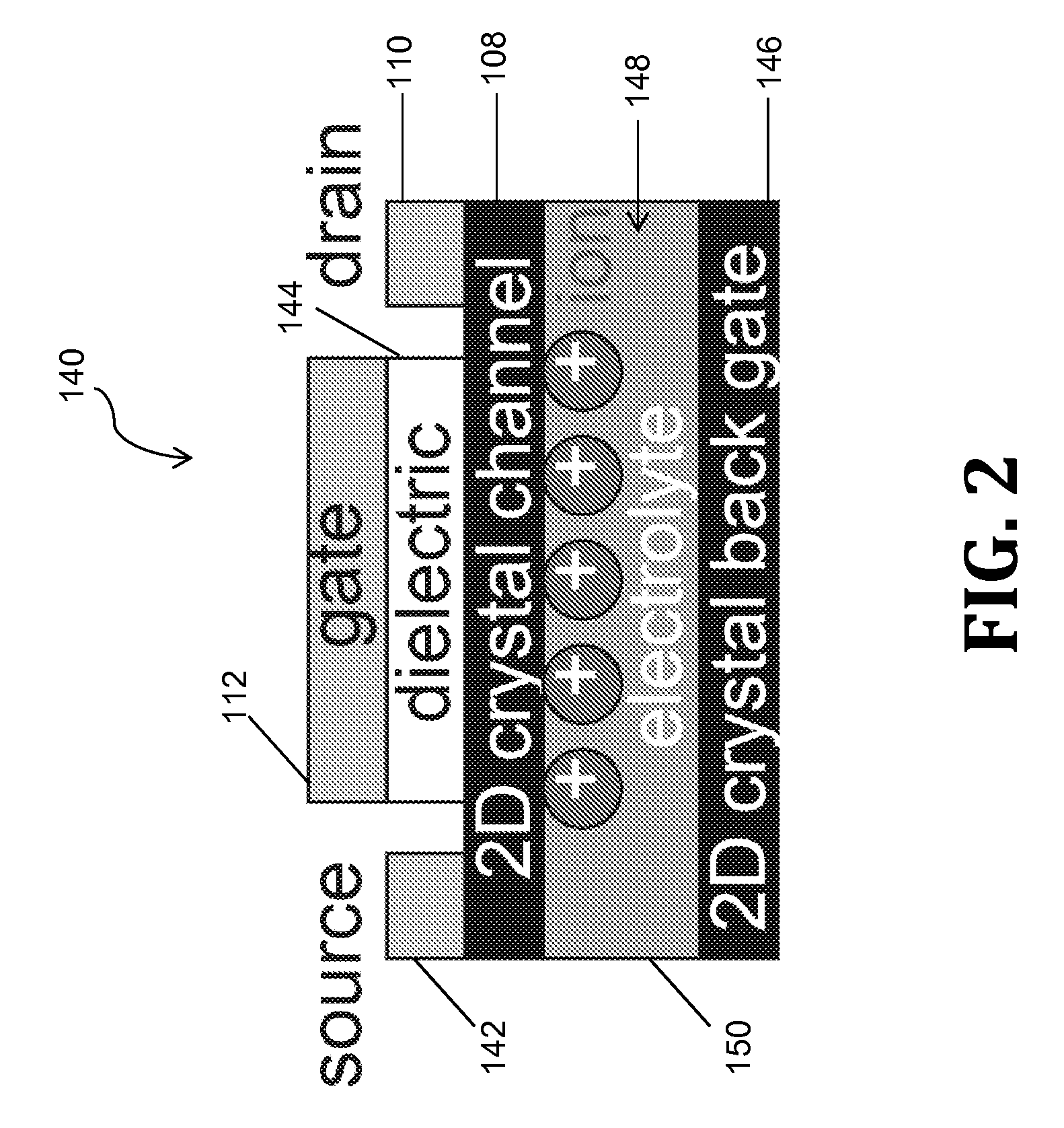
[0012]An example single-transistor random access memory (RAM) cell is disclosed for high-density data storage on two-dimensional (2D) crystals like graphene, for example. It will be appreciated that any 2D crystal or other similar structure may be utilized as desired. In one example, a data storage mechanism is contained within a specialized transistor. The transistor may function as a memory without the need for an added storage capacitor or resistance-change element, allowing for a device of atomic proportions. In one example, the single-transistor RAM cell includes a bit line, a word line, and a write line. Similar to flash memory, the bit line and word line may be used to address the 2D crystal transistor in an arr...


PUM


Abstract

A single-transistor random access memory (RAM) cell may be used as universal memory. The single-transistor RAM cell generally includes a first gate, a 2D-crystal channel, a source, a drain, an ion conductor, and a second (back) gate. The single-transistor RAM cell is capable of drifting ions towards the graphene channel. The ions in turn induce charge carriers from the source into the graphene channel. The closer the ions are to the graphene channel, the higher the conductivity of the graphene channel. As the ions are spaced from the graphene channel, the conductivity of the graphene channel is reduced. Thus the presence of the charged ions adjacent to the channel is used to modify the channel's conductivity, which is sensed to indicate the state of the memory.

Description

CROSS REFERENCE TO RELATED APPLICATION[0001]This application is a non-provisional application claiming priority from U.S. Provisional Application Ser. No. 61 / 852,318, filed Mar. 15, 2013, and incorporated herein by reference in its entirety.FIELD OF THE DISCLOSURE[0002]The present disclosure relates generally to a universal memory. More particularly, the present disclosure relates to a random access memory cell formed by a transistor incorporating ion storage and a two-dimensional crystal.BACKGROUND OF RELATED ART[0003]Nonvolatile memory retains stored data even when power is not supplied to the memory. Nonvolatile memory devices are currently widely employed in computers, mobile communication terminals, memory cards, and the like. There are various types of nonvolatile memories, such as, for example, flash memory. Generally, flash memory includes memory cells typically having a stacked gate structure. The stacked gate structure may include a tunnel oxide layer, a floating gate, an ...

Claims


Application Information

Patent Timeline
IPC IPC(8): H01L27/11H01L29/16
CPCH01L29/1606H01L27/11G11C13/0016G11C13/0014G11C2213/53H10K85/20H10K10/482H10K10/20
Inventor SEABAUGH, ALANFULLERTON, SUSAN
Owner UNIV OF NOTRE DAME DU LAC
Why Eureka
Try Eureka