Antenna for plasma generation, plasma processing apparatus and plasma processing method

a plasma processing apparatus and plasma technology, applied in the direction of plasma technique, antenna, electric discharge tube, etc., can solve the problems of difficult to provide a plasma processing technique that can adequately meet the demands of finer micro-fabrication of semiconductor elements, and the plasma temperature of plasma generated in inductively coupled plasma processing apparatus or capacitively coupled plasma processing apparatus is rather high

Active Publication Date: 2014-11-20
TOKYO ELECTRON LTD
View PDF9 Cites 224 Cited by
  • Summary
  • Abstract
  • Description
  • Claims
  • Application Information

AI Technical Summary

Benefits of technology

[0011]According to an aspect of the present invention, an antenna for plasma generation, a plasma processing apparatus, and a plasma processing method may be provided for supplying a microwave and gas.

Problems solved by technology

However, the electron temperature of plasma generated in an inductively coupled plasma processing apparatus or a capacitively coupled plasma processing apparatus is rather high.
Also, a region with an adequately high plasma density is rather limited.
Thus, it has been difficult to provide a plasma processing technique that can adequately meet the demands of finer micro-fabrication of semiconductor elements.

Method used


Image

  • Antenna for plasma generation, plasma processing apparatus and plasma processing method
  • Antenna for plasma generation, plasma processing apparatus and plasma processing method
  • Antenna for plasma generation, plasma processing apparatus and plasma processing method

Examples


Embodiment Construction

[0028]In the following, embodiments of the present invention are described with reference to the accompanying drawings. Note that elements having substantially the same functions or features may be given the same reference numerals and overlapping descriptions thereof may be omitted.

[0029][Overall Configuration of Plasma Processing Apparatus]

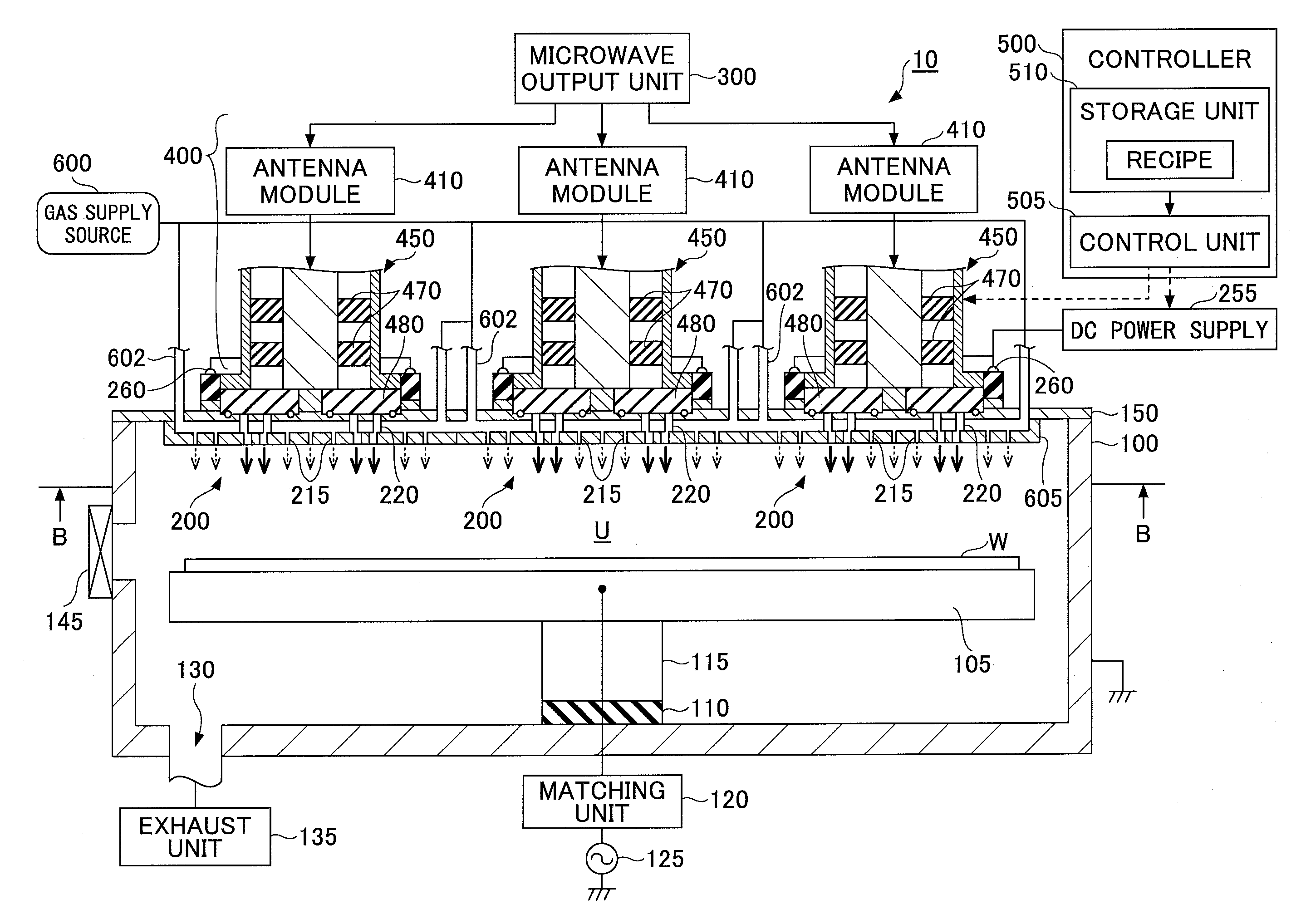
[0030]First, an overall configuration of a plasma processing apparatus 10 according to an embodiment of the present invention is described with reference to FIG. 1. FIG. 1 is a longitudinal cross-sectional view of the plasma processing apparatus 10 according to the present embodiment.

[0031]The plasma processing apparatus 10 of the present embodiment is configured as a plasma etching apparatus for performing an etching process as a plasma process on a semiconductor wafer W (simply referred to as “wafer W” hereinafter). The plasma processing apparatus 10 includes a substantially cylindrical airtight processing chamber 100 in which a plasma process...


PUM


Abstract

An antenna for plasma generation radiates a microwave transmitted through a coaxial waveguide into a processing chamber and propagates the microwave on a metal surface of the processing chamber to convert gas into surface wave plasma. The antenna includes a gas flow path for passing the gas through the antenna, a plurality of gas holes that communicate with the gas flow path and introduce the gas into the processing chamber, and a plurality of slots that are separated from the gas flow path and penetrate through the gas flow path. The slots pass the microwave transmitted through the coaxial waveguide and a slow-wave plate to the processing chamber. A first space between portions of adjacent slots penetrating through the gas flow path is arranged to be wider than a second space between portions of the adjacent slots opening out to a plasma generation space of the processing chamber.

Description

TECHNICAL FIELD[0001]The present invention relates to an antenna for plasma generation, a plasma processing apparatus, and a plasma processing method.BACKGROUND ART[0002]Plasma processing is an indispensable technique for manufacturing semiconductor devices. In view of the growing demand for higher and faster integration of large-scale integrated circuit (LSI) devices in recent years, there is a demand for techniques that enable finer micro-fabrication of semiconductor elements making up the LSI. However, the electron temperature of plasma generated in an inductively coupled plasma processing apparatus or a capacitively coupled plasma processing apparatus is rather high. Also, a region with an adequately high plasma density is rather limited. Thus, it has been difficult to provide a plasma processing technique that can adequately meet the demands of finer micro-fabrication of semiconductor elements.[0003]To meet such demands for finer micro-fabrication of semiconductor elements, gen...

Claims


Application Information

Patent Timeline
Patent Type & Authority Applications(United States)
IPC IPC(8): H01J37/32
CPCH01J37/3222H01J2237/006H01J37/32449H01J37/32229H01J37/3244H05H1/46H05H1/4615H05H1/463
Inventor KOMATSU, TOMOHITOIKEDA, TAROKASAI, SHIGERU
Owner TOKYO ELECTRON LTD
Why Eureka
Try Eureka