Unlock instant, AI-driven research and patent intelligence for your innovation.

Variable-gain dual-output transconductance amplifier-based instrumentation amplifiers

a transconductance amplifier and amplifier technology, applied in differential amplifiers, amplifiers with semiconductor devices/discharge tubes, amplifiers, etc., can solve problems such as distortion of cmos transmission gate switches

Active Publication Date: 2014-11-20
HONEYWELL INT INC
View PDF2 Cites 0 Cited by
  • Summary
  • Abstract
  • Description
  • Claims
  • Application Information

AI Technical Summary

Benefits of technology

The present invention provides an instrumentation amplifier that has a variable-gain without causing distortion. This amplifier includes two current conveyors, a resistive element, and an amplifier. The resistive element can be adjusted to change the gain of the amplifier. The current conveyors are also called dual-output trans conductance amplifiers (DOTAs). The technical effect of this invention is that it provides a way to accurately measure small voltages without introducing distortion, which can be caused by transmission gates.

Problems solved by technology

CMOS transmission gate (T-gate) switches introduce distortion when used in an instrumentation amplifier (IA).

Method used


Image

  • Variable-gain dual-output transconductance amplifier-based instrumentation amplifiers
  • Variable-gain dual-output transconductance amplifier-based instrumentation amplifiers
  • Variable-gain dual-output transconductance amplifier-based instrumentation amplifiers

Examples


Embodiment Construction

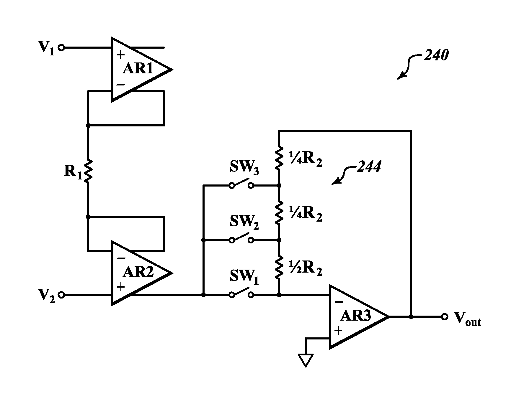
[0010]FIG. 2 illustrates an instrumentation amplifier (IA) 20. For clarity, dual-output transconductance amplifier (DOTA) symbols 26, 28 are used to represent current conveyors. One of ordinary skill would understand how to apply current conveyors to the IA 20. The gain of the IA 20 is defined by the following equation:

AV=VOUT / (V1-V2)=R2 / R1  (1)

[0011]As shown in FIG. 3, a IA 40 includes an additional resistor, R3, between resistor R1 and the DOTA 26. The voltage gain remains the same, Av =R2 / R1, because there is no significant current flowing through the resistor R3, especially when using CMOS amplifiers, and no voltage is developed across the resistor R3.

[0012]Also in the IA 40, a resistor R4 is added between the resistor R1 and the DOTA 26. The gain remains the same for small values of the resistor R4. In this case, the same current that flows through the resistor R1 also flows through the resistor R4 but the voltage that develops across the resistor R4 does not affect overall gai...


PUM


Abstract

A variable-gain current conveyor-based instrumentation amplifier without introducing distortion. An exemplary variable-gain instrumentation amplifier includes a first dual-output transconductance amplifier (DOTA) (i.e., current conveyor) that receives a first input voltage, a second DOTA that receives a second input voltage, a first resistive element connected between the first and second DOTA, an amplifier connected to the second DOTA at an inverting input, and a second resistive element that connects the second DOTA and the inverting input to an output of the amplifier. At least one of the resistive elements is a variable resistive element.

Description

BACKGROUND OF THE INVENTION[0001]CMOS transmission gate (T-gate) switches introduce distortion when used in an instrumentation amplifier (IA). A prior-art transmission gate circuit is shown in FIG. 1. Transistors MN1 and MP1 form the CMOS switch between pins “IN” and “OUT”. This switch is controlled by the “PGATE” and “NGATE” voltages, which are driven out of phase and rail to rail (0-5V) by two digital inverters.[0002]The off-resistance of this switch is essentially infinite (>1000 meg). The on-resistance is typically between 50 and 5000 ohms, depending on design, and varies with process, supply voltage, and temperature (PVT). Furthermore, the on-resistance also varies with the voltage present at the “IN” and “OUT” terminals. The magnitude of this non-linear variation in resistance is typically significant, on the order of + / −10% of the nominal on-resistance over the full range of applied voltages in a given system. In amplifier circuits where low signal distortion is important,...

Claims


Application Information

Patent Timeline
Patent Type & Authority Applications(United States)
IPC IPC(8): H03G3/00
CPCH03G3/00H03F1/3211H03F3/45475H03F2200/261H03F2203/45138H03F2203/45522H03F2203/45528H03G1/0035H03G1/0088
Inventor WERKING, PAUL M.
Owner HONEYWELL INT INC