Transfer printing substrate, manufacturing method thereof, and method of transfer printing

a technology of transfer printing and substrate, applied in the field of transfer printing, can solve the problems of reducing alignment, reducing transfer yield, and reducing transfer yield, so as to achieve stable bonding force, high transfer yield and alignment, and minimize damage to an element

Active Publication Date: 2014-11-27
GWANGJU INST OF SCI & TECH
View PDF2 Cites 3 Cited by
  • Summary
  • Abstract
  • Description
  • Claims
  • Application Information

AI Technical Summary

Benefits of technology

[0010]An object of the present invention is to provide a transfer printing substrate capable of implementing high transfer yield and alignment and maintaining stable bonding force between a handling substrate and an ultra-thin film substrate while minimizing damage to an element by using a pillar structure and a sacrificial layer.

Problems solved by technology

However, in the case in which the thickness of the substrate is reduced to several tens micrometers, the substrate is likely to be twisted or bent during a manufacturing process.
However, in the case in which the sacrificial layer is removed by an etching solution, the ultra-thin film substrate on the handling substrate floats and deviates from an original position, thereby decreasing alignment, or the ultra-thin film substrate immersed during an etching process is strongly bonded to the handling substrate, thereby decreasing the transfer yield.
There are problems in that the etching solution vulnerable to damage is used, a floating phenomenon of the pattern is caused due to a long etching time, it is costly, it is likely to be damaged by heat, and so forth.

Method used


Image

  • Transfer printing substrate, manufacturing method thereof, and method of transfer printing
  • Transfer printing substrate, manufacturing method thereof, and method of transfer printing
  • Transfer printing substrate, manufacturing method thereof, and method of transfer printing

Examples


Embodiment Construction

[0041]Hereinafter, exemplary embodiments of the present invention will be described in detail with reference to the accompanying drawings. When it is determined that the detailed description of the known art related to the present invention may obscure the gist of the present invention, the detailed description thereof will be omitted.

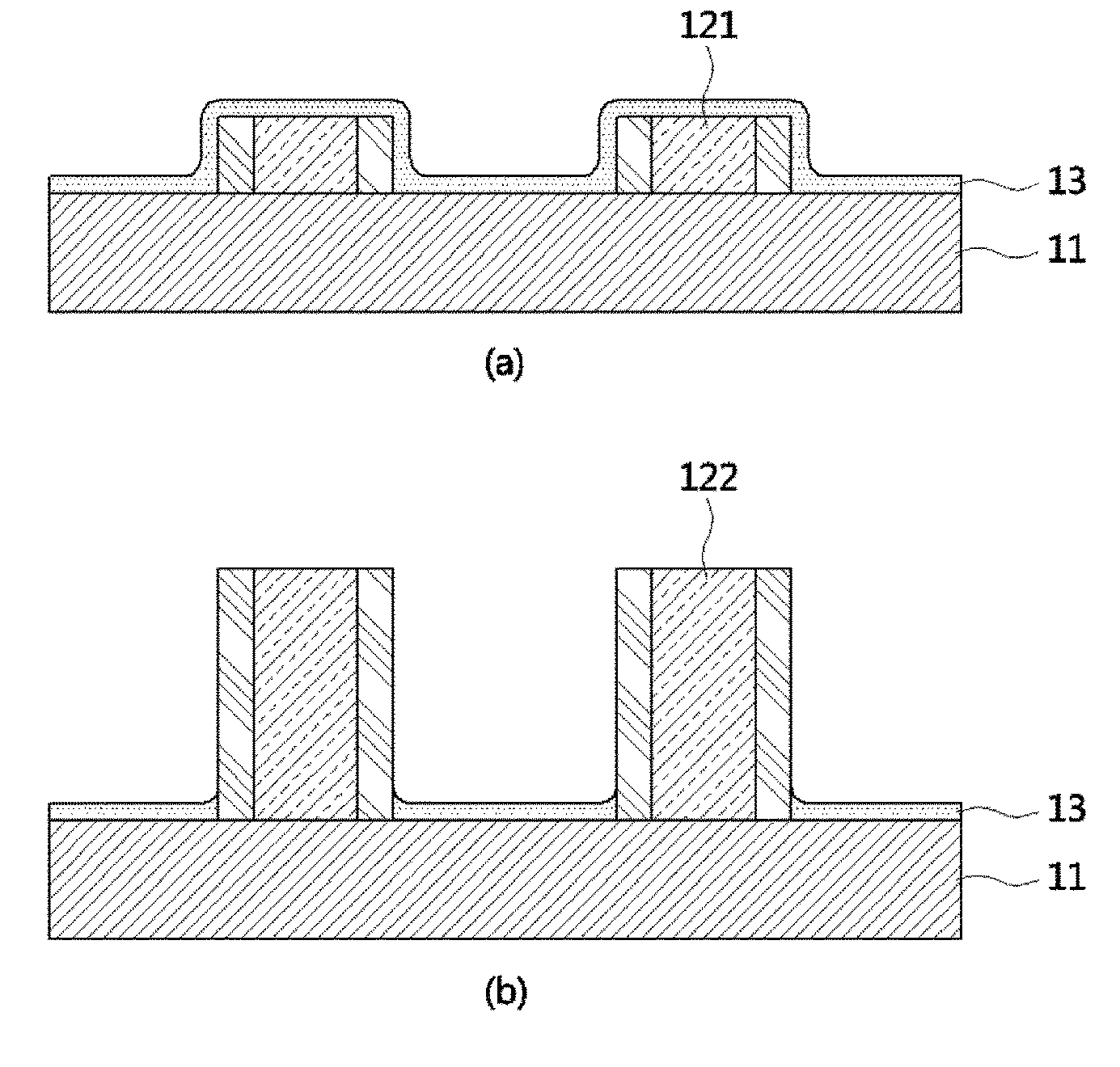
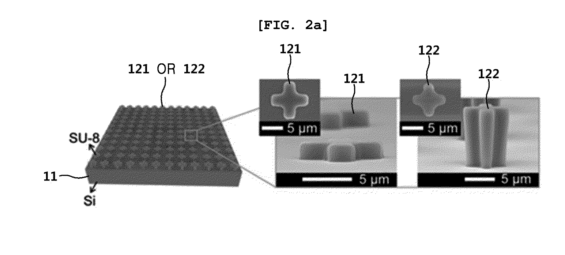
[0042]First, briefly describing, according to the present invention, the polymer is coated on a handling substrate, for example, a silicon wafer using a spin coating and a plurality of pillar structures are then formed by a photolithography process. In this case, in order to increase bonding force between the handling substrate and the polymer pillar structure, after the polymer is coated in a film form, the pillar structure may be formed thereon. A sacrificial layer is applied on an upper layer of the handling substrate having the plurality of pillar structures formed thereon, using various methods such as a spray coating method, a spin coating method...


PUM

PropertyMeasurementUnit
heightaaaaaaaaaa
heightsaaaaaaaaaa
heightsaaaaaaaaaa

Abstract

Disclosed herein is a transfer printing technology. A transfer printing substrate includes a plurality of pillar structures and a sacrificial layer applied thereon. In situ alignment of a transfer layer is performed by the pillar structures and a structural confinement by a concave structure formed on a bottom surface of the transfer layer corresponding to the pillar structures, or a chemical bond of the pillar structure and the transfer layer. In the in situ alignment by the structural confinement, the remaining sacrificial layer after being removed may serve as an adhesive component. The transfer process is performed by a separation of the bond by the sacrificial layer, a cutting of the pillar structures in the chemic bonding state of the pillar structures and the transfer layer, or a separation of the bond between the pillar structures and the handling substrate.

Description

CROSS REFERENCE TO RELATED APPLICATION[0001]This application claims the benefit of Korean Patent Application No. 10-2013-0057147, filed on May 21, 2013, which is hereby incorporated by reference in its entirety into this application.BACKGROUND OF THE INVENTION[0002]1. Technical Field[0003]The present invention relates to a transfer printing field, and more particularly, to a transfer printing substrate capable of implementing high alignment and transfer rate even in a case of an ultra-thin film element by using a pillar structure, a manufacturing method thereof, and a method of transfer printing.[0004]2. Description of the Related Art[0005]Future electric and electronic elements need to have shape variability. For example, the reason is that the elements may be required to repeatedly deform shapes thereof such as clothes or human body organs, or may be attached to a building outer wall having various forms of surfaces in a deformed shape to thereby be maintained. Mechanical flexibil...

Claims


Application Information

Patent Timeline
Patent Type & Authority Applications(United States)
IPC IPC(8): B41F16/00B41M5/025
CPCB41M5/025B41F16/00H01L2924/0002Y10T428/24174H10K71/13H10K71/80H10K71/00H01L2924/00H01L21/0273H01L21/3205H01L29/66477H05K3/20
Inventor KO, HEUNG CHOYUN, SU OKPARK, JEONG PILKIM, SUK HOHWANG, YOUNG KYUHYUN, YUJUNJANG, HUN SOOJEONG, YUN KYUNG
Owner GWANGJU INST OF SCI & TECH
Why Eureka
Try Eureka