Apparatus for the processing of single molecules

a technology of apparatus and single molecules, applied in the field of apparatus and a single molecule processing method, can solve the problems of high electrical conductivity of graphene layer, small conductivity change induced by a molecule, and mechanically inability of associated apparatus, etc., to prevent the flow of undesired electrical current, reduce the effect of asymmetry and small apertur

Active Publication Date: 2014-11-27
KONINKLJIJKE PHILIPS NV
View PDF3 Cites 30 Cited by
  • Summary
  • Abstract
  • Description
  • Claims
  • Application Information

AI Technical Summary

Benefits of technology

[0020]The first slit in the bottom layer and the second slit in the top layer are arranged one above the other such that they commonly yield the desired aperture. In general, it is possible that one slit is completely overlapped by the other (e.g. if both slits are identical in size and shape and exactly aligned). The resulting aperture would then correspond in size and shape to this (smaller) slit. Though such an embodiment shall be comprised by the invention, it is preferred that the first slit and the second slit do not completely overlap. The aperture, which always corresponds to the region of overlap between the slits, will then be smaller than each of the slits alone. This design is favorable in that a small aperture can be more easily produced with the help of comparatively large apertures (the slits).
[0021]The first and the second slit may have elongated (e.g. rectangular) shapes that are oriented coaxially with a relative shift in axial direction. Hence, only a smaller area where these slits overlap will constitute the aperture. Most preferably, the two slits are however oriented oblique with respect to each other, particularly perpendicular. In this case the exact relative position of the slits can largely vary, allowing for large production tolerances, without affecting the size and shape of the resulting aperture.
[0022]The first and / or the second slit may be completely surrounded by the corresponding layer (being an interior opening of said layer), it may have a connection to one border of the layer, or it may cut the layer into two disconnected parts. The latter case may preferably be realized for the top layer and the second slit. The two parts of the top layer are then electrically disconnected, yielding zero background currents across the second slit. Most preferably, this is combined with a first slit that lies completely in the interior of its layer and thus provides a mechanically stable, one-piece bottom layer.
[0023]The top layer is optionally provided with an electrical insulation on at least a part of its surface, preferably on its whole surface besides at the aperture and / or the second slit. The electrical insulation prevents the flow of undesired electrical currents, particularly currents between two disconnected parts of the top layer that are separated by the second slit (cf. aforementioned embodiment). Thus only currents through a region of interest are generated (i.e. typically currents across the second slit), while currents through the surrounding sample medium and / or through other components of the apparatus (e.g. the bottom layer) are prevented or at least minimized.

Problems solved by technology

One drawback of this sensor is the high electrical conductivity of the graphene layer, compared to which conductivity changes induced by a molecule are very small.
The associated apparatus is, however, mechanically not very robust as free graphene layers are used.
Moreover, the comparatively long gap between said layers allows long molecules to pass it with many different orientations and configurations, making the interpretation of measurement results difficult.

Method used


Image

  • Apparatus for the processing of single molecules
  • Apparatus for the processing of single molecules
  • Apparatus for the processing of single molecules

Examples


Embodiment Construction

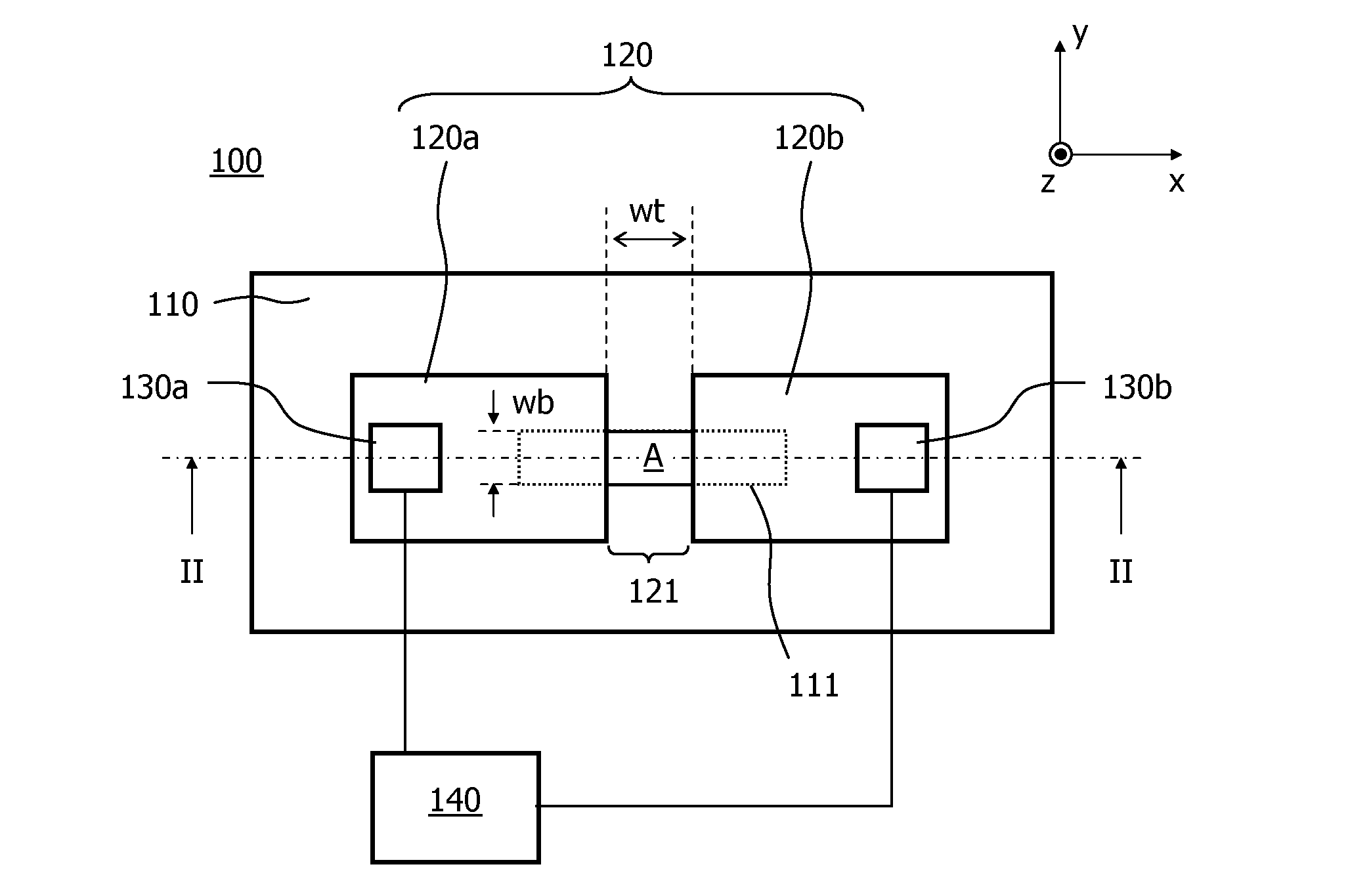
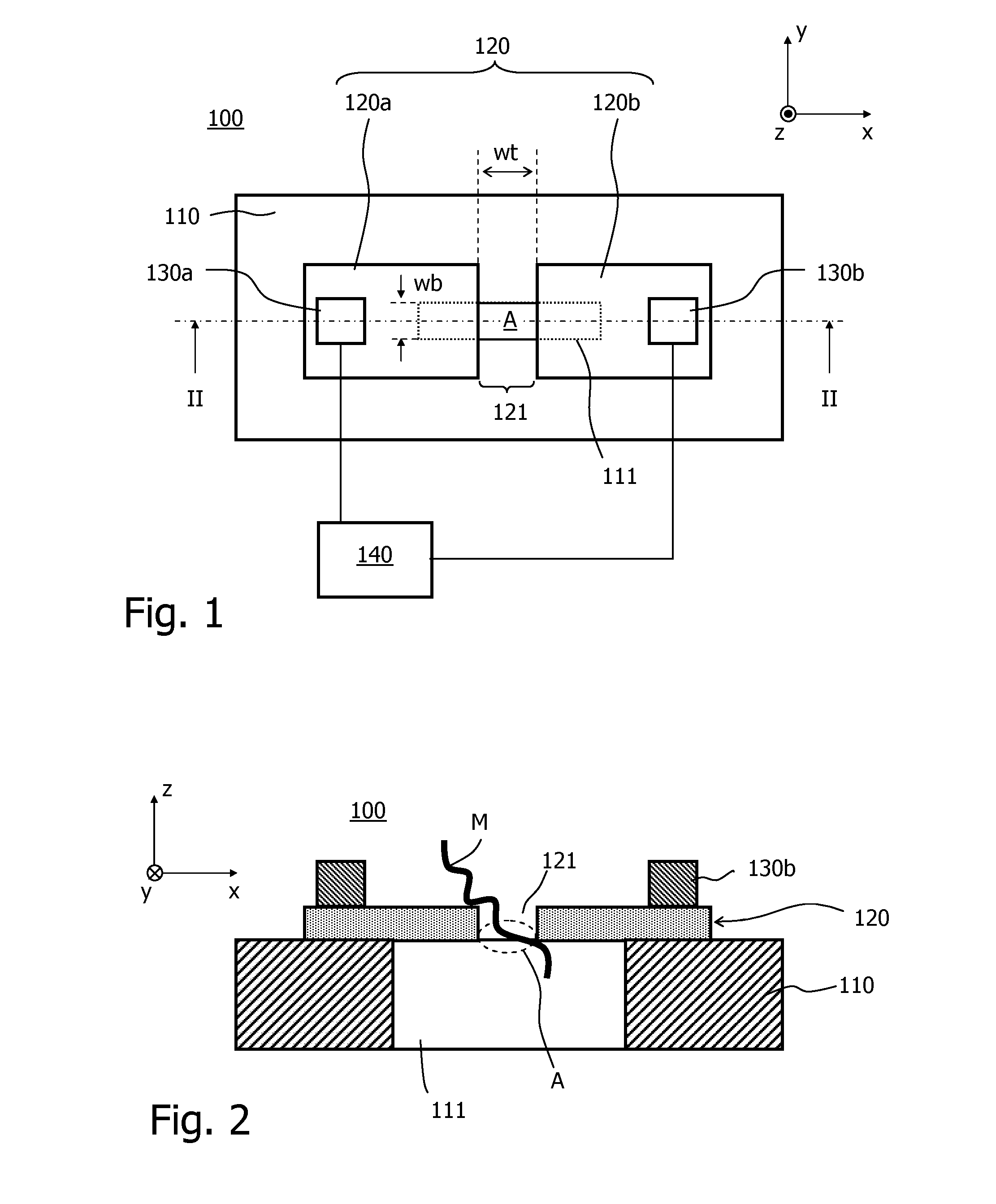
[0044]The U.S. 2010 / 0327847 A1 describes the use of a graphene layer / electrode in nanopore sequencing. It is proposed in this patent that a nanopore is embedded in the graphene, leaving areas besides the nanopore.

[0045]However, it is already known that graphene has a very high conductivity. A mobility of around 10,000 cm2 / Vs at room temperature has been reported (K. S. Novoselov, A. K. Geim, S. V. Morozov, D. Jiang, Y. Zhang, S. V. Dubonos, I. V. Grigorieva, and A. A. Firsov, “Electric Field Effect in Atomically Thin Carbon Films”, Science, 306 (204) 666-669). Hence, the current in the device of the U.S. 2010 / 0327847 A1 will not or only hardly be modulated and the devices will have a poor effectiveness in determining the bases passing through the nanopore, as nearly all of the current will pass by the nanopore in the remaining graphene.

[0046]In view of this, it seems to be more effective to use nanogaps, as proposed by Postma (H. W. Ch. Postma, “Rapid sequencing of individual DNA mo...


PUM

PropertyMeasurementUnit
thicknessaaaaaaaaaa
thicknessaaaaaaaaaa
widthaaaaaaaaaa

Abstract

The invention relates to an apparatus(100) and a method for the processing of single molecules, particularly for the sensing or sequencing of single-stranded DNA. A bottom layer(110) and an electrically conductive top layer(120) with a first and a second slit(111,121), respectively, are disposed on top of each other such that an aperture(A) is formed by the slits. The slits(111,121) are preferably perpendicular to each other. An electrical circuit(140) may be connected to the top layer(120), allowing to sense single molecules that pass through the aperture(A).

Description

FIELD OF THE INVENTION[0001]The invention relates to an apparatus and a method for the processing of single molecules. Moreover, it relates to a method for manufacturing such an apparatus.BACKGROUND OF THE INVENTION[0002]The U.S. 2010 / 0327847 A1 discloses a solid state molecular sensor having an aperture extending through a graphene layer. A change in an electrical characteristic of said layer is measured when a molecule passes through said aperture. One drawback of this sensor is the high electrical conductivity of the graphene layer, compared to which conductivity changes induced by a molecule are very small.[0003]Furthermore, it has been described in literature (H. W. Ch. Postma, “Rapid sequencing of individual DNA molecules in graphene nanogaps”, Nano Lett. 10 (2010) 420-425) that a DNA molecule can be sequenced by passing it through a gap between two graphene layers. The associated apparatus is, however, mechanically not very robust as free graphene layers are used. Moreover, t...

Claims


Application Information

Patent Timeline
Patent Type & Authority Applications(United States)
IPC IPC(8): G01N33/487
CPCG01N33/48721
Inventor VAN DER ZAAG, PIETER JANCOEHOORN, REINDERVAN DELFT, FALCO CORNELIUS MARINUS JACOBUS MARIA
Owner KONINKLJIJKE PHILIPS NV
Why Eureka
Try Eureka