
Isolation structure and method for forming the same, and image sensor including the isolation structure and method for fabricating the image sensor

a technology of isolation structure and isolation structure, which is applied in the direction of material analysis, radiofrequency controlled devices, instruments, etc., can solve problems such as deterioration in device characteristics, and achieve the effect of reducing the refractive index of the amorphous impurity region

Active Publication Date: 2014-12-04
SK HYNIX INC
View PDF3 Cites 17 Cited by
  • Summary
  • Abstract
  • Description
  • Claims
  • Application Information

AI Technical Summary

Benefits of technology

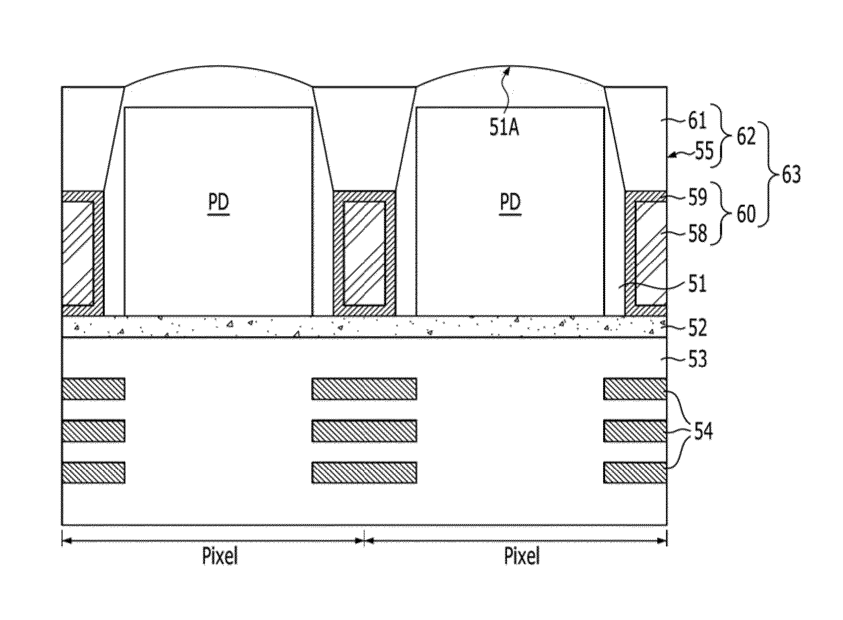
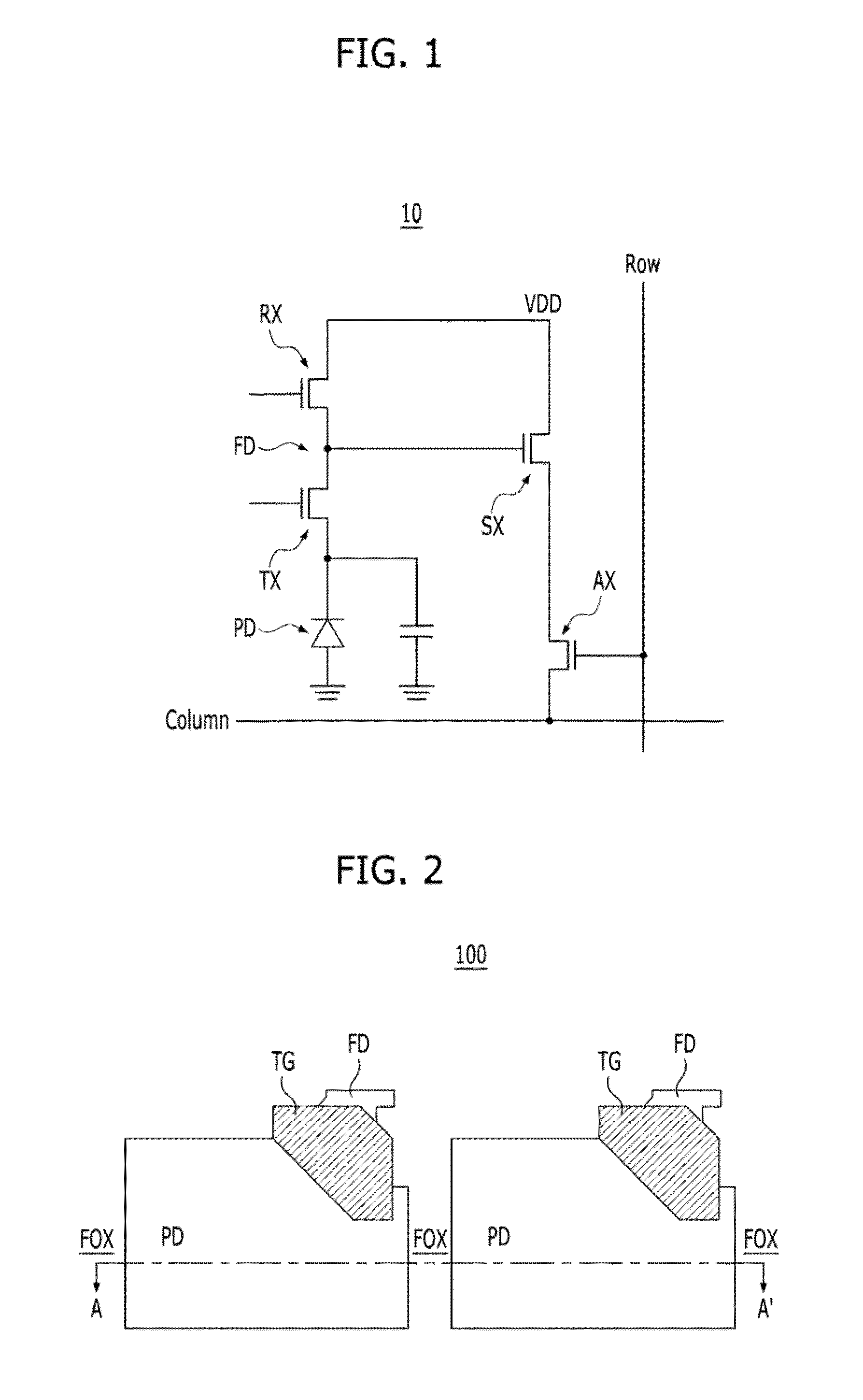
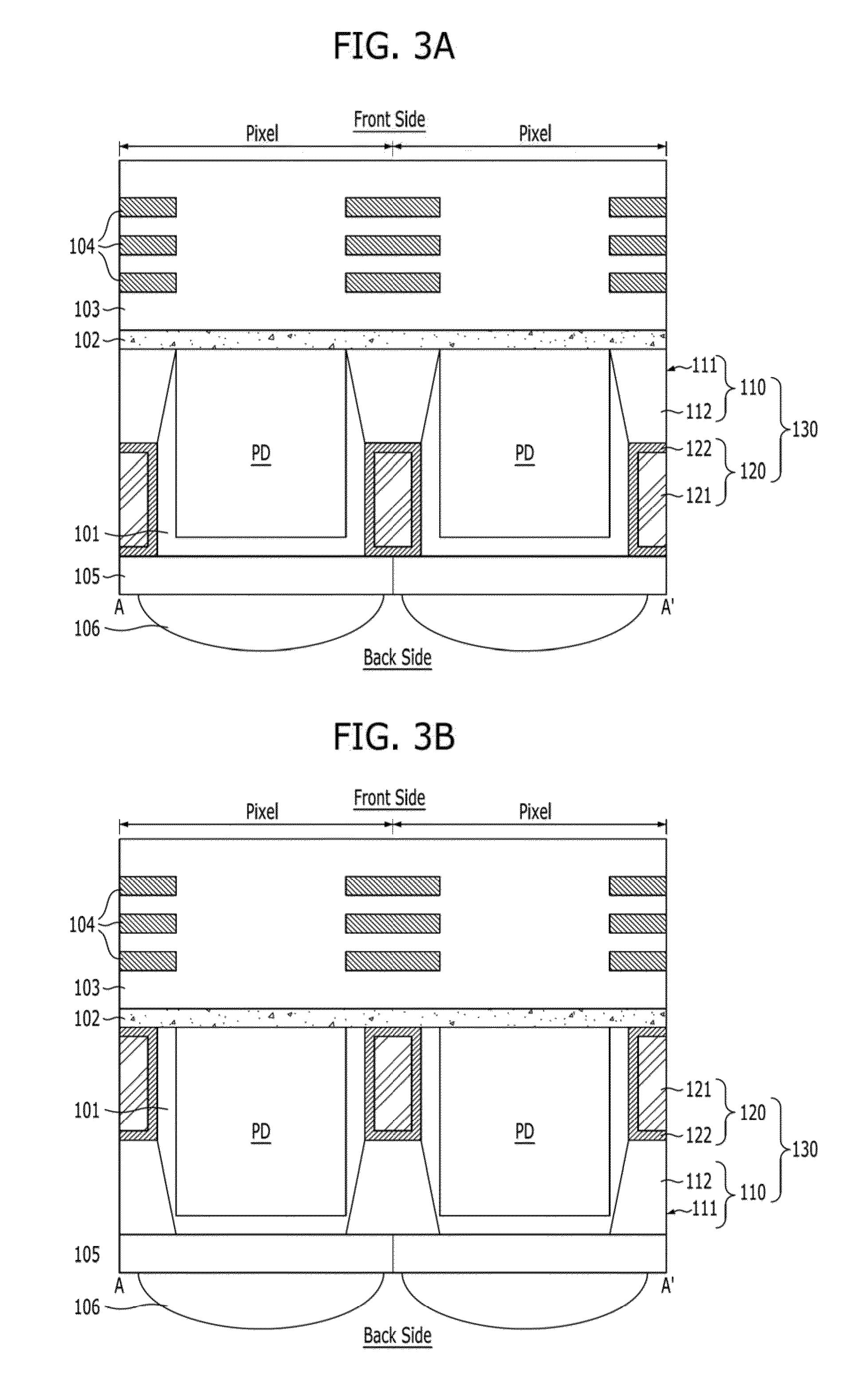
The patent describes an isolation structure for a semiconductor device that includes a trench filled with insulation material and a second isolation structure formed on top of the first isolation structure. The second isolation structure includes a first impurity region with a lower doping concentration and a second impurity region with a higher doping concentration. The method for forming the isolation structure includes etching the substrate to form the trench, implanting an impurity into the substrate, and performing an annealing process to activate the impurity. The isolation structure can be used in image sensors to prevent cross-talk between pixels. The technical effect of the invention is to improve the performance and reliability of semiconductor devices.

Problems solved by technology

The reduction in space between the pixels may lead to deterioration in device characteristics because of the crosstalk between the pixels.

Method used


Image

  • Isolation structure and method for forming the same, and image sensor including the isolation structure and method for fabricating the image sensor
  • Isolation structure and method for forming the same, and image sensor including the isolation structure and method for fabricating the image sensor
  • Isolation structure and method for forming the same, and image sensor including the isolation structure and method for fabricating the image sensor

Examples


Embodiment Construction

[0043]Exemplary implementations of the present invention will be described below in more detail with reference to the accompanying drawings. The present invention may, however, be embodied in different forms and should not be construed as limited to the implementations set forth herein. Rather, these implementations are provided so that this disclosure will be thorough and complete, and will fully convey the scope of the present invention to those skilled in the art. Throughout the disclosure, reference numerals correspond directly to the like numbered parts in the various figures and embodiments of the present invention.

[0044]The drawings are not necessarily to scale and in some instances, proportions may have been exaggerated in order to clearly illustrate features of the implementations. It should be readily understood that the meaning of “on” and “over” in the present disclosure should be interpreted in the broadest manner such that “on” means not only “directly on” but also “on...


PUM


Abstract

An isolation structure and method of forming the same. The isolation structure includes a first isolation structure having including an insulation layer formed in a trench in a substrate and a second isolation structure, formed on the first isolation structure. The second isolation structure includes a first impurity region formed in the substrate, the first impurity region having a first impurity doping concentration, and a second impurity region that is formed around the first impurity region, the second impurity region having a second impurity doping concentration that is greater than the first doping concentration.

Description

CROSS-REFERENCE TO RELATED APPLICATIONS[0001]The present application claims priority of Korean Patent Application Nos. 10-2013-0062477 and 10-2003-0062478, filed on May 31, 2013, which are incorporated herein by reference in their entirety.BACKGROUND[0002]1. Field[0003]Exemplary implementations of the present invention relate to a semiconductor device fabrication technology, and more particularly, to an isolation structure and a method for forming the isolation structure, and an image sensor including the isolation structure and a method for fabricating the image sensor.[0004]2. Description of the Related Art[0005]An image sensor is a semiconductor device that transforms an optical image into electrical signals. Image sensors may be divided into a Charge Coupled Device (CCD) type and a Complementary Metal Oxide Semiconductor (CMOS) type. The CMOS-type image sensors are commonly abbreviated as “CIS.” A CIS may include a plurality of pixels that are arrayed in two dimensions, and each...

Claims


Application Information

Patent Timeline
IPC IPC(8): H01L27/146H01L29/06
CPCH01L27/1463H01L29/0649H01L29/0646H01L27/1464H01L27/14643
Inventor CHOI, CHUNG-SEOKMOON, JANG-WONKIM, JONG-CHAEKIM, DO-HWANRO, KYOUNG-OUG
Owner SK HYNIX INC
Learn More