
Eureka
For R&D, Eureka makes reading and utilizing patents & technical documents easy.
Eureka AIR
Designed for self-driven R&D workflows. Generate viable solutions, solve complex R&D challenges, empower your innovation with AI.

Eureka Materials
Designed for material experts only. Revolutionize your material R&D, from search, analyze, to developing new materials.

TechResearch
Generate reliable direction feasibility study reports for your R&D in just a few steps.

TechSeek
Discover and master advanced knowledge NOW. Basics, ideas, possibilities, all at once.

TechMind
As an expert in R&D Theories, TechMind can generates customized viable solutions instantly.

TechRisk
Analyze your overall solution with one click, know your potential R&D risks in advance.

TechMonitor
Get weekly tech updates, stay abreast of the latest tech innovations and key insights.
Gas supply method for semiconductor manufacturing apparatus, gas supply system, and semiconductor manufacturing apparatus
- Summary
- Abstract
- Description
- Claims
- Application Information
AI Technical Summary
Benefits of technology
Problems solved by technology
Method used
Image

Examples
application example
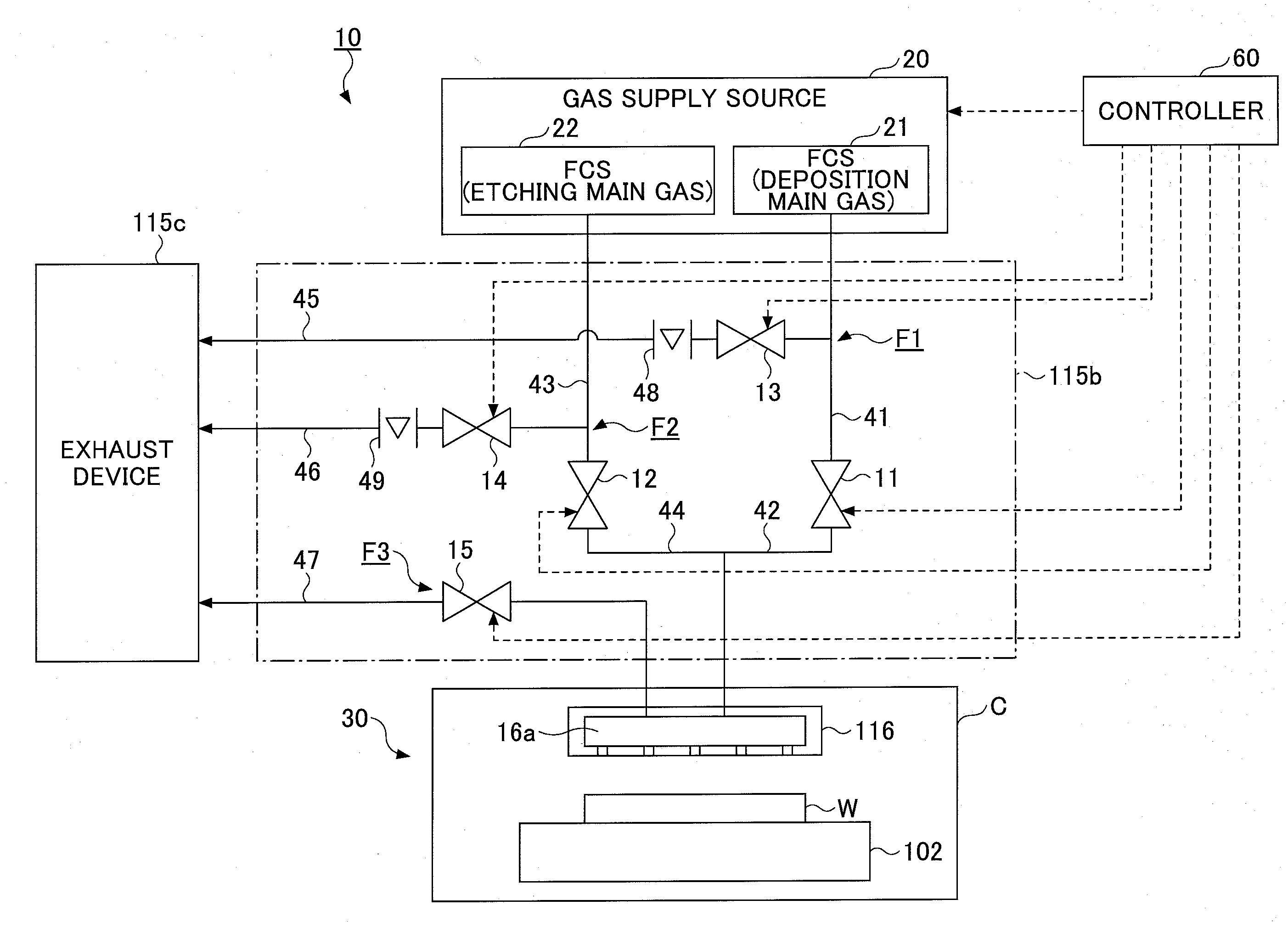
[0144]Note that an etching process for forming a deep hole in the silicon substrate W using the gas supply system 10 according to the present embodiment has been described above as an illustrative example. In the following, an application example of the present embodiment is described with reference to FIG. 14.
[0145]In the application example, the semiconductor manufacturing apparatus 30 according to the present embodiment is used in 3D circuitization for establishing electrical connection between semiconductor chips stacked on one another using an electrode of a through hole (TSV: through-silicon via) penetrating through a semiconductor chip. In FIG. 14, a through hole (TSV) 405 is formed in an upper semiconductor chip 400. Wiring is passed through the through hole 405 to cause a pad electrode 410 of the upper semiconductor chip 400 and a pad electrode 510 of a lower semiconductor chip 500 to conduct with each other via the through hole 405 and a bump 505.
[0146]In the present examp...
PUM
 Abstract
Description
Claims
Application Information
 - R&D Engineer
- R&D Manager
- IP Professional
- Industry Leading Data Capabilities
- Powerful AI technology
- Patent DNA Extraction
Browse by: Latest US Patents, China's latest patents, Technical Efficacy Thesaurus, Application Domain, Technology Topic, Popular Technical Reports.
© 2024 PatSnap. All rights reserved.Legal|Privacy policy|Modern Slavery Act Transparency Statement|Sitemap|About US| Contact US: help@patsnap.com