
Process for producing at least one through-silicon via with improved heat dissipation, and corresponding three-dimensional integrated structure

a technology of through-silicon and heat dissipation, which is applied in the direction of semiconductor devices, semiconductor/solid-state device details, electrical apparatus, etc., can solve the problems of limiting the operating power of integrated circuits and therefore their performance, and achieve the effect of improving the heat dissipation of through-silicon

Active Publication Date: 2014-12-11
STMICROELECTRONICS INT NV
View PDF3 Cites 13 Cited by
  • Summary
  • Abstract
  • Description
  • Claims
  • Application Information

AI Technical Summary

Benefits of technology

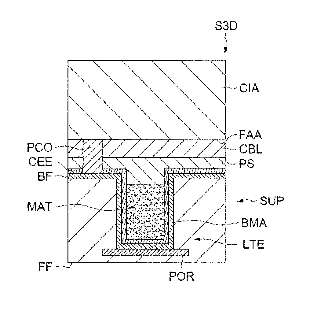
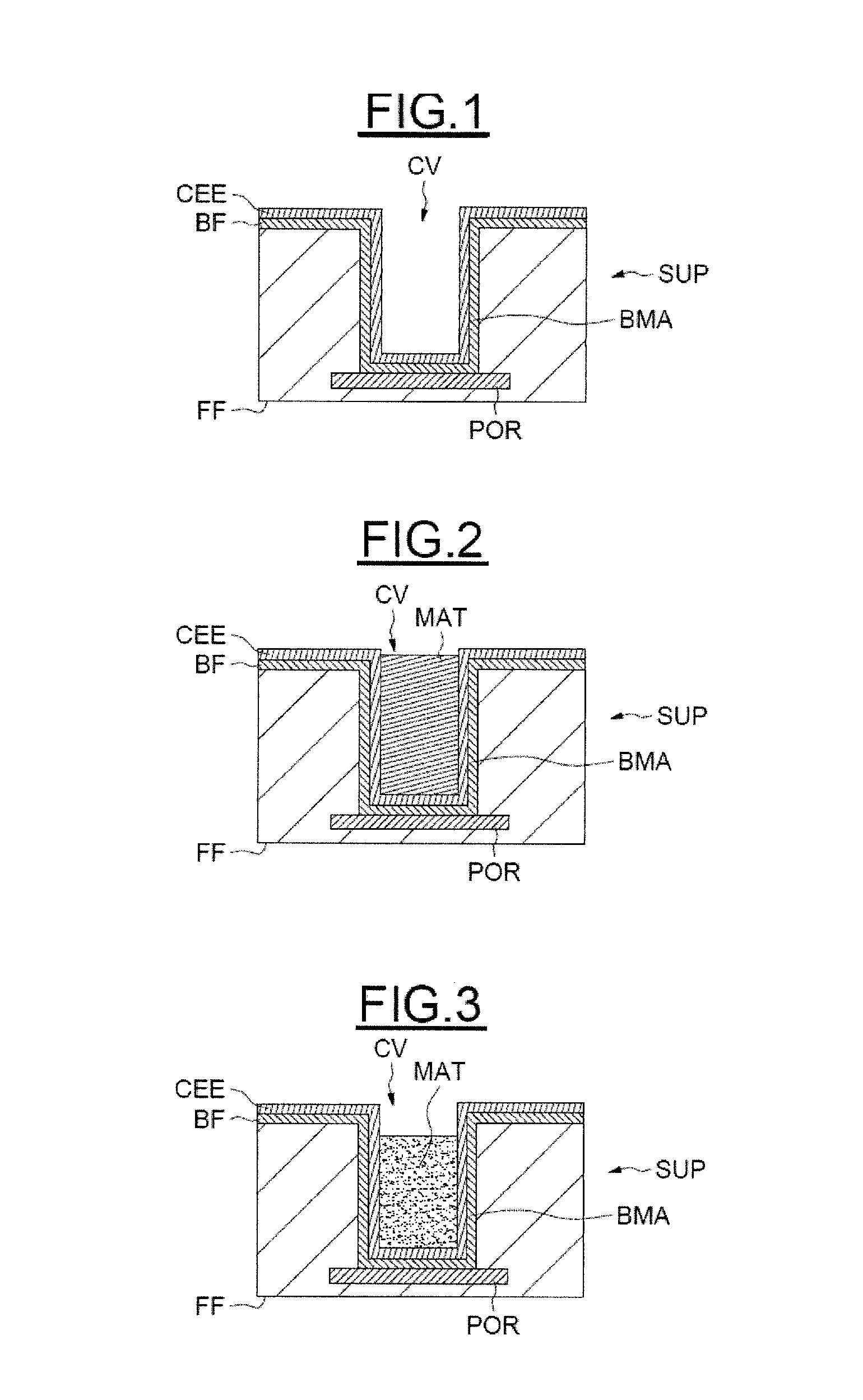
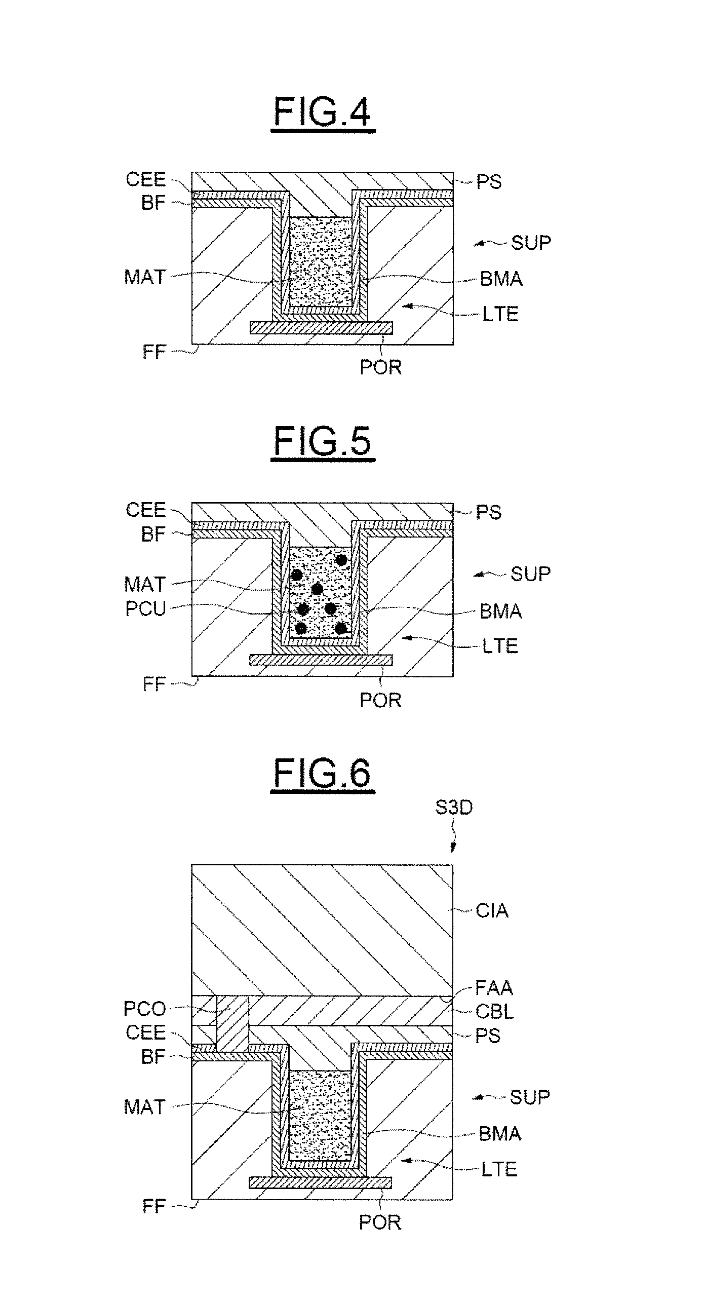
The patent is about a method and structure for improving heat dissipation in a three-dimensional integrated structure. The method involves making changes to the through-silicon vias, which form barriers to heat dissipation, and at least partially filling them with a phase-change material. This helps to store and release thermal energy during operation, thereby improving heat dissipation. The process also involves adding an insulating layer to prevent electrical contact between the material and a conductive material. The cavity is filled with a layer of flexible polymer to protect the phase-change material and ensure its stability during packaging. Additionally, the cavity may be filled with a phase-change material containing copper particles to increase its thermal conductivity. Overall, this method and structure improve the heat dissipation and protect the integrated circuit from excessive heat.

Problems solved by technology

This heat generally limits the operating power of the integrated circuits and therefore their performance.

Method used


Image

  • Process for producing at least one through-silicon via with improved heat dissipation, and corresponding three-dimensional integrated structure
  • Process for producing at least one through-silicon via with improved heat dissipation, and corresponding three-dimensional integrated structure
  • Process for producing at least one through-silicon via with improved heat dissipation, and corresponding three-dimensional integrated structure

Examples


Embodiment Construction

[0019]FIG. 1 shows a substrate SUP, for example, a silicon wafer. The substrate SUP may include a region that includes components, for example transistors, forming the Front End Of Line (FEOL) region well known to those skilled in the art. The substrate SUP may also include a Back End Of Line (BEOL) region that includes an electrically conductive portion POR. The electrically conductive portion POR is produced in the vicinity of the front side FF of the substrate.

[0020]The substrate SUP also includes a back side BF opposite the front side FF. To assemble an integrated circuit to the back side BF of the substrate SUP, an electrical connection is formed between this back side and the metallic lines arranged in the vicinity of the front side FF of the substrate SUP, for example the portion POR.

[0021]For this purpose, a cavity CV can be formed that extends into the substrate SUP from the back side BF as far as the electrically conductive portion POR. Formation of the cavity may be follo...


PUM


Abstract

A method for producing at least one through-silicon via inside a substrate may include forming a cavity in the substrate from a first side of the substrate until an electrically conductive portion is emerged onto. The method may also include forming an electrically conductive layer at a bottom and on walls of the cavity, and at least partly on a first side outside the cavity. The process may further include at least partially filling the cavity with at least one phase-change material. Another aspect is directed to a three-dimensional integrated structure.

Description

FIELD OF THE INVENTION[0001]The invention relates to integrated circuits, particularly three-dimensional integrated structures comprising through-silicon vias, and more particularly to heat dissipation inside such structures.BACKGROUND OF THE INVENTION[0002]Three-dimensional integrated structures generally comprise at least two integrated circuits fabricated independently then connected together. Conventionally, to connect the back side of a first integrated circuit to the front side of a second integrated circuit, through-silicon vias are produced inside the first integrated circuit.[0003]During operation of these integrated circuits, the various components of the integrated circuits release heat. This heat generally limits the operating power of the integrated circuits and therefore their performance.[0004]U.S. Pat. No. 7,666,768 describes through-silicon vias that include carbon structures to decrease thermal expansion of the through-silicon vias and increase electrical conductiv...

Claims


Application Information

Patent Timeline
Patent Type & Authority Applications(United States)
IPC IPC(8): H01L23/373H01L23/48H01L21/768
CPCH01L23/3736H01L23/481H01L21/76898H01L23/3677H01L23/4275H01L24/16H01L24/73H01L2224/16235H01L2224/73204
Inventor BAR, PIERREGOUSSEAU, SIMONBEILLIARD, YANN
Owner STMICROELECTRONICS INT NV
Learn More