

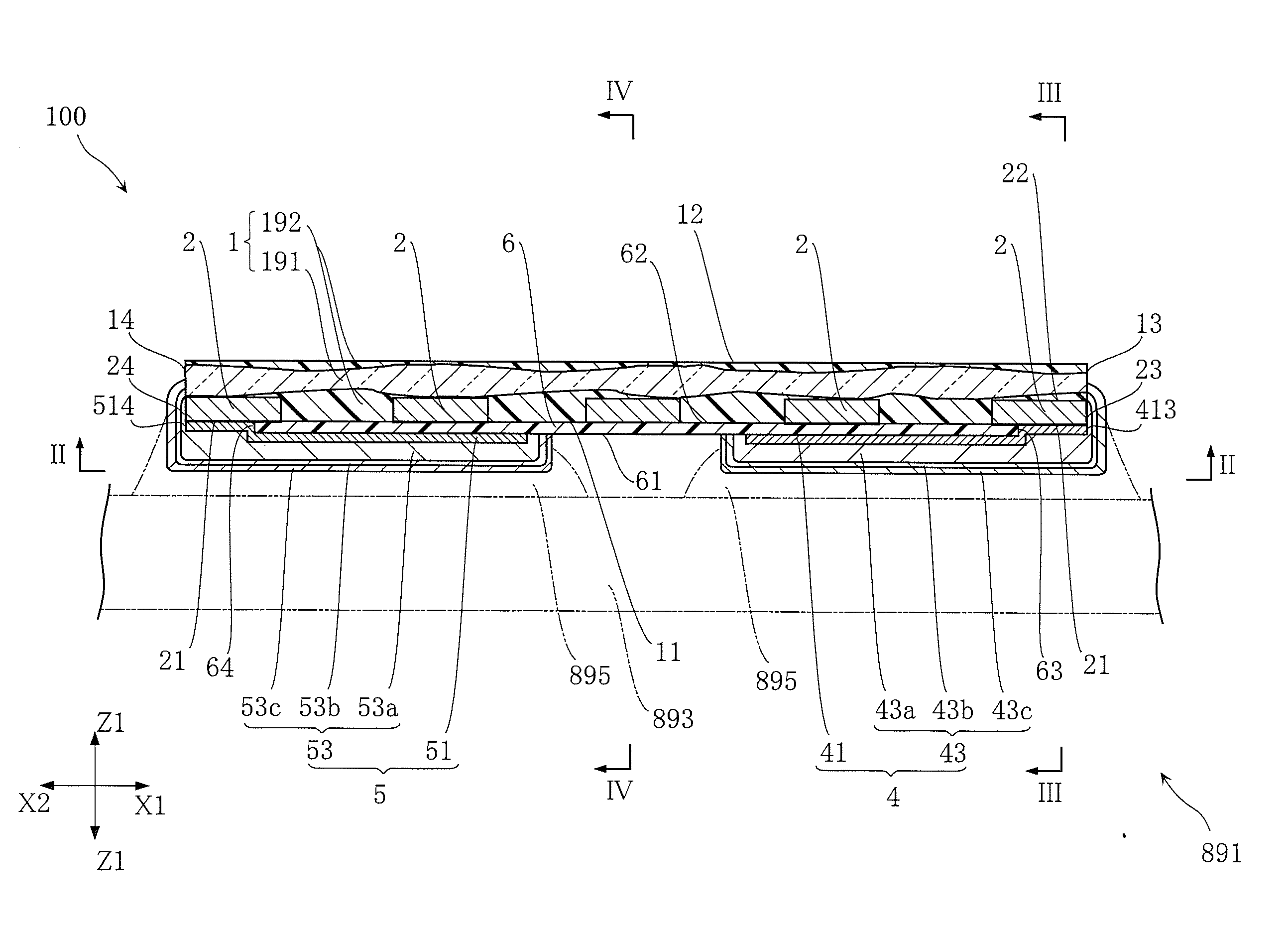
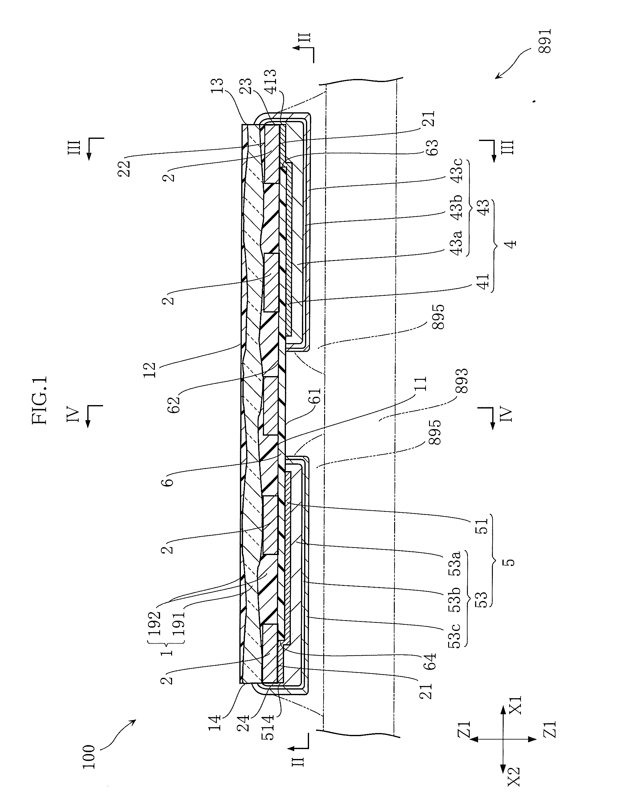
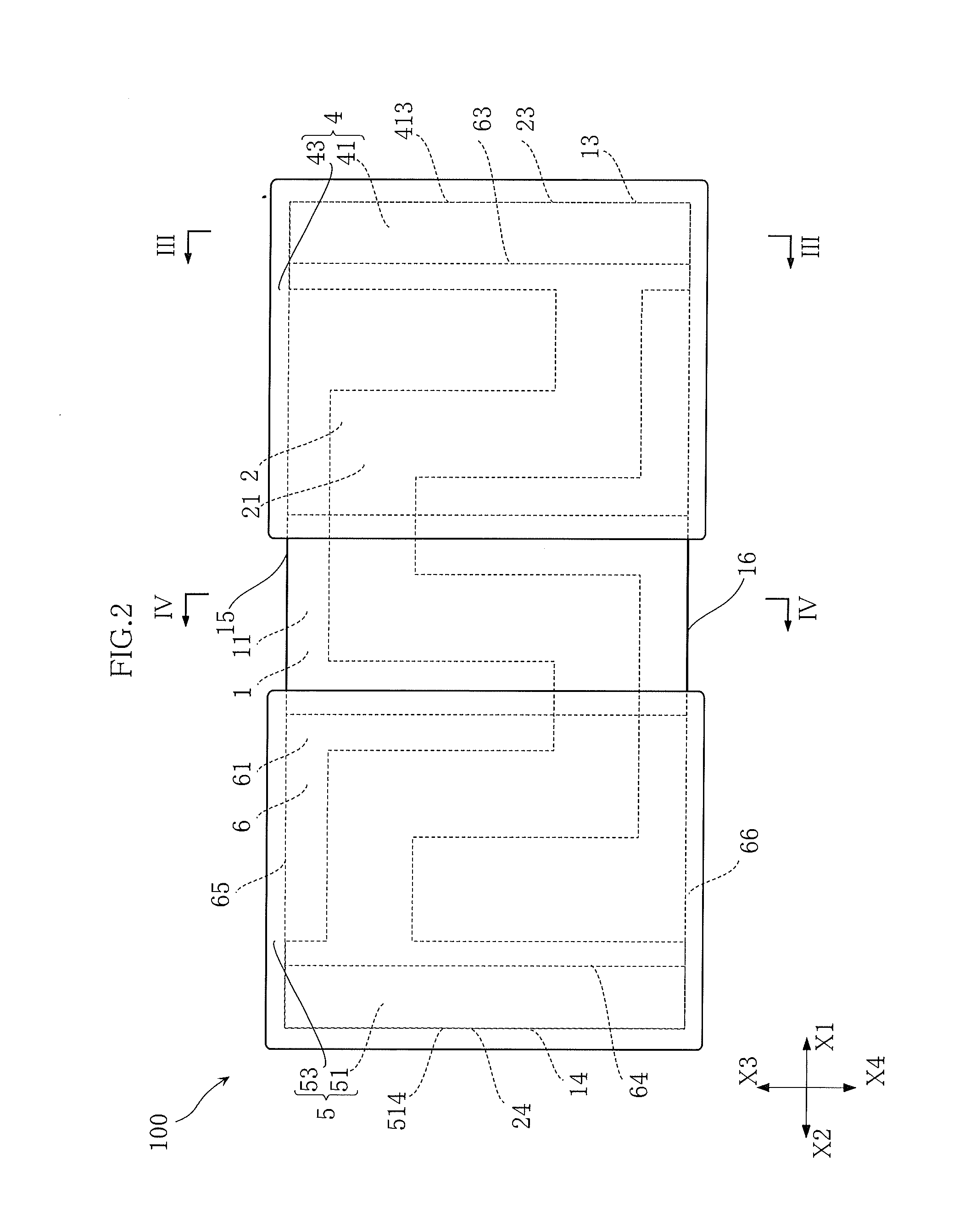
Chip resistor and mounting structure thereof
- Summary
- Abstract
- Description
- Claims
- Application Information
AI Technical Summary
Benefits of technology
Problems solved by technology
Method used
Image

Examples
first embodiment
First Variation of First Embodiment
[0116]Referring to FIG. 18, a first variation of the first embodiment of the present invention will be described.
[0117]FIG. 18 is a cross-sectional view showing the first variation of the first embodiment.
[0118]A chip resistor 101 shown in FIG. 18 is different from the chip resistor 100 in that the resistor first lateral face 23 and the resistor second lateral face 24 of the resistor 2 are covered with the substrate 1. The remaining portions are configured in the same way as those of the chip resistor 100, and hence the description will not be repeated.
[0119]The chip resistor 101 can also provide the same advantages as those provided by the chip resistor 100.
[0120]Referring to FIG. 19, a second variation of the first embodiment of the present invention will be described.
[0121]FIG. 19 is a cross-sectional view showing the second variation of the first embodiment.
[0122]A chip resistor 102 shown in FIG. 19 is different from the chip resistor 100 in th...
second embodiment
Second Variation of Second Embodiment
[0175]Referring to FIG. 39, a second variation of the second embodiment of the present invention will be described.
[0176]FIG. 39 is a cross-sectional view showing the second variation of the second embodiment.
[0177]A chip resistor 202 shown in FIG. 39 is different from the chip resistor 200 in that the first plated layer 43 includes a face that is flush with the underlying layer first lateral face 413 of the first underlying layer 41, and that the second plated layer 53 includes a face that is flush with the underlying layer first lateral face 514 of the second underlying layer 51. The remaining portions are configured in the same way as those of the chip resistor 200, and hence the description will not be repeated. Here, to manufacture the chip resistor 202, the plated layer is formed in advance of the cutting process of the substrate sheet 810 and the resistor block 820 described with reference to FIGS. 36 and 37.
[0178]The chip resistor 202 can...
PUM
 Abstract
Description
Claims
Application Information