Method of manufacturing semiconductor device, substrate processing apparatus and non-transitory computer-readable recording medium

a technology of semiconductor devices and processing equipment, which is applied in the direction of liquid surface applicators, chemical vapor deposition coatings, coatings, etc., can solve the problems of reducing film forming productivity, difficult to set the concentration of carbon (c) in the bcn film to a predetermined concentration, and complicated control of the three types of gases, so as to increase the controllability of the concentration of carbon (c) and increase the productivity of boron carbonitrid

Active Publication Date: 2014-12-18
KOKUSA ELECTRIC CO LTD
View PDF3 Cites 1 Cited by
  • Summary
  • Abstract
  • Description
  • Claims
  • Application Information

AI Technical Summary

Benefits of technology

[0007]It is an object of the present invention to increase the controllability of the concentration of carbon (C) contained in a boron carbonitride (BCN) film or a boron nitride (BN) film by increasing the productivity of forming the boron carbonitride (BCN) film or the boron nitride (BN) film.

Problems solved by technology

However, controlling the three types of gases is complicated, and film-forming productivity may decrease when the above-described technique is used.
In addition, it may be difficult to set the concentration of carbon (C) in the BCN film to a predetermined concentration when the above-described technique is used.

Method used


Image

  • Method of manufacturing semiconductor device, substrate processing apparatus and non-transitory computer-readable recording medium
  • Method of manufacturing semiconductor device, substrate processing apparatus and non-transitory computer-readable recording medium
  • Method of manufacturing semiconductor device, substrate processing apparatus and non-transitory computer-readable recording medium

Examples


first embodiment

of the Present Invention

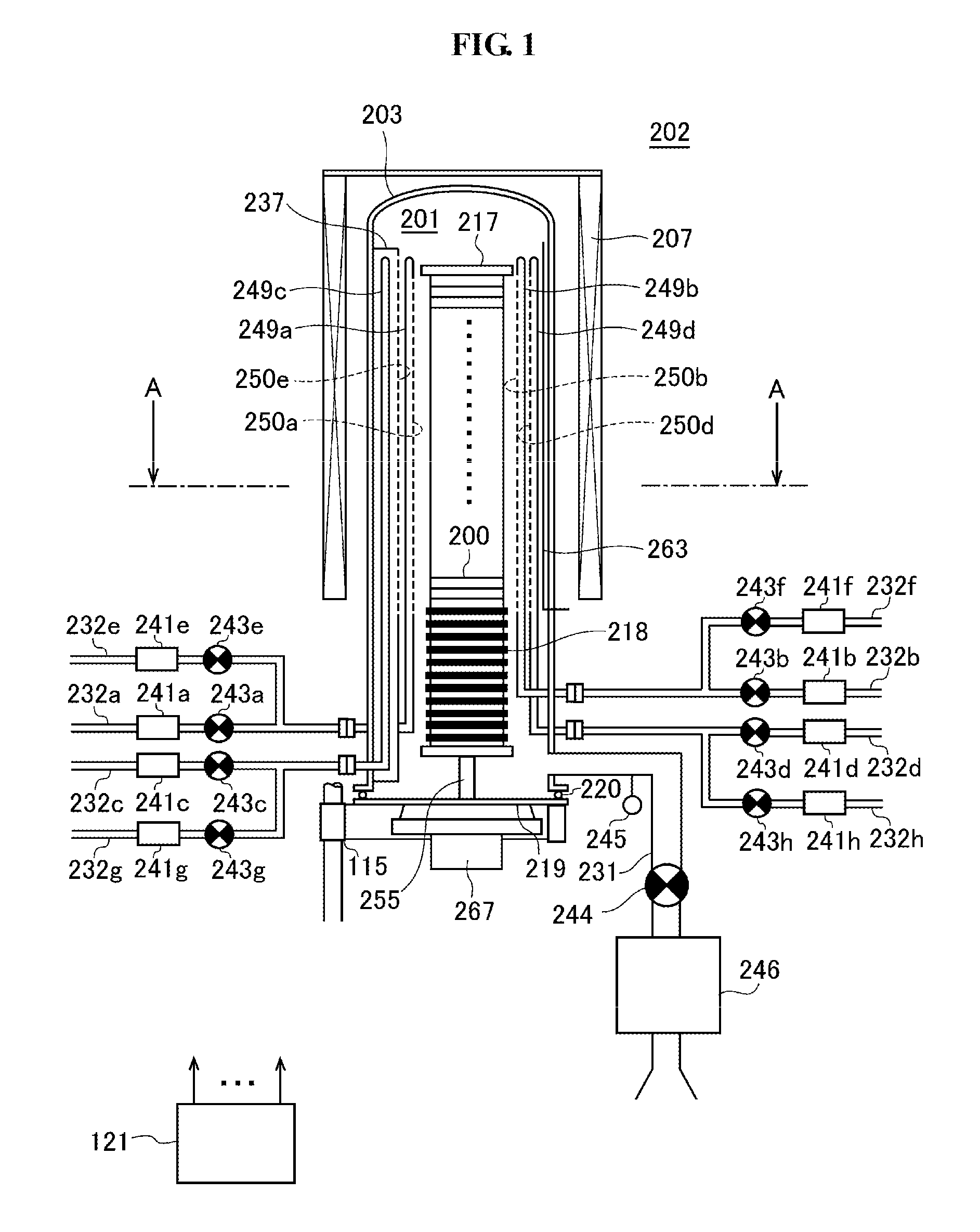
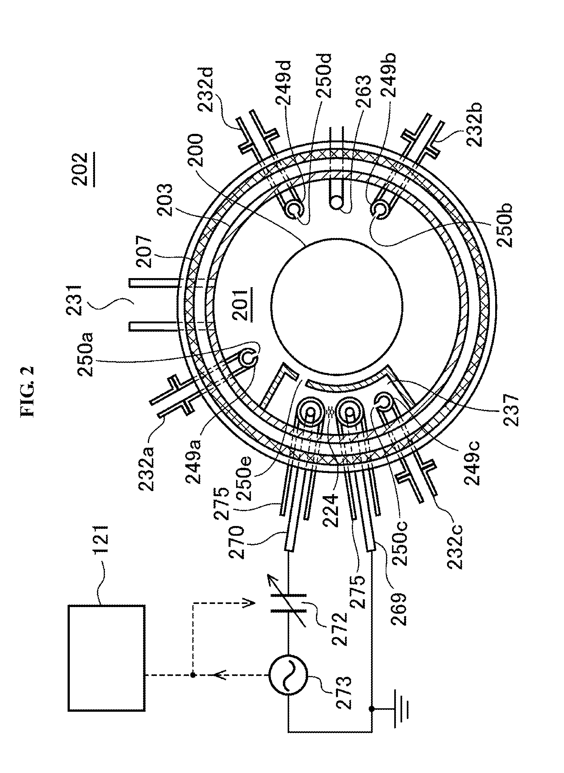
[0026]Hereinafter, a first embodiment of the present invention will be described with reference to FIGS. 1 through 3.

[0027](1) Structure of Substrate Processing Apparatus

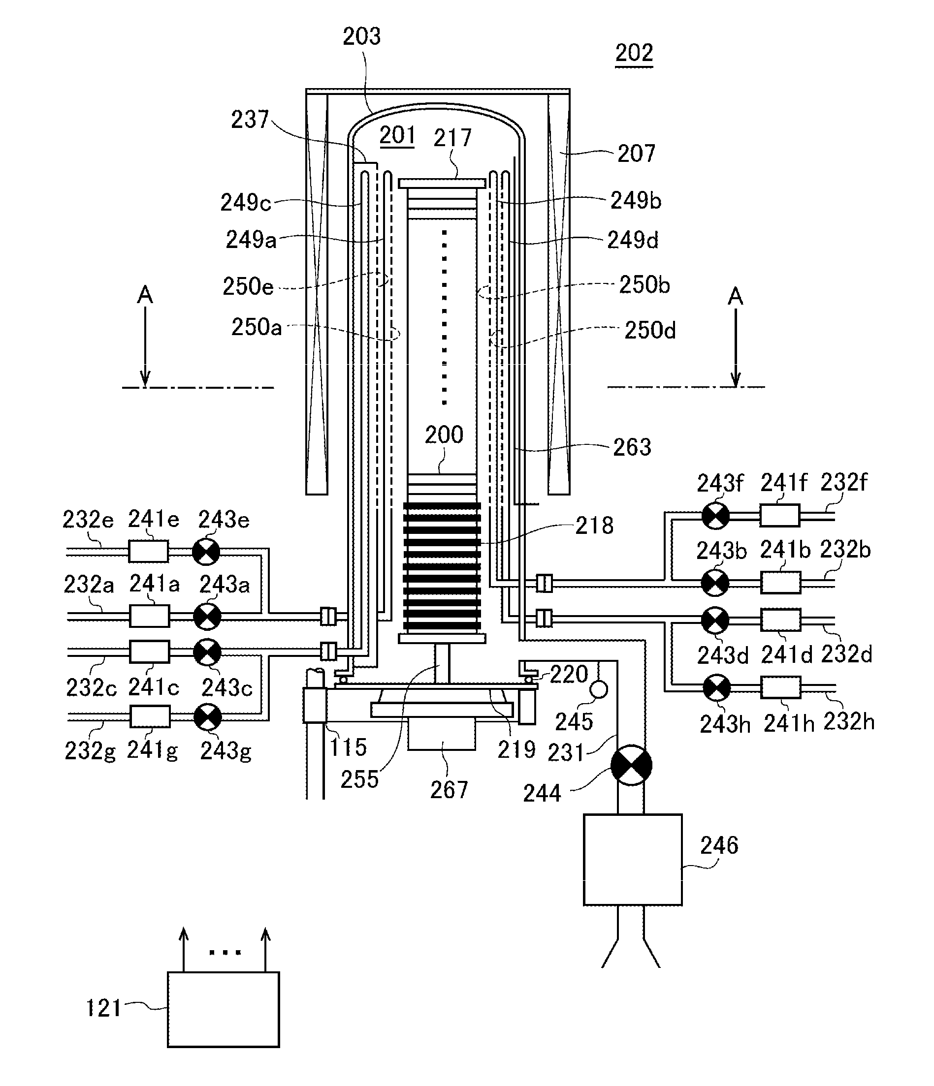
[0028]As illustrated in FIG. 1, a process furnace 202 includes a heater 207 serving as a heating unit (heating mechanism). The heater 207 has a cylindrical shape and is vertically installed by being supported by a heater base (not shown) serving as a retaining plate. The heater 207 also acts as an activating mechanism (excitation unit) that activates a gas with heat as will be described below.

[0029]In the heater 207, a reaction tube 203 forming a reaction container (process container) in a concentric shape with the heater 207 is provided. The reaction tube 203 is formed of a heat-resistant material, e.g., quartz (SiO2) or silicon carbide (SiC), and has a cylindrical shape, an upper end of which is closed and a lower end of which is open. A process chamber 201 is formed in a hollow tubular por...

second embodiment

of the Present Invention

[0145]Next, a second embodiment of the present invention will be described below.

[0146]In the above-described first embodiment, a case in which the cycle including steps 1a and 2a is performed a predetermined number of times to form a BCN film on a substrate has been described. In the present embodiment, a case in which a BCN film or a BN is formed on a substrate by performing a predetermined number of times a cycle including not only steps 1b and 2b (which are similar to steps 1a and 2a described above) but also step 3b of supplying a nitriding gas to the substrate will be described.

[0147](First Sequence)

[0148]First, a first sequence according to the present embodiment will be described with reference to FIGS. 6 and 7.

[0149]In the first sequence according to the present embodiment, a cycle including a process of supplying a chloroborane-based source gas (e.g., BCl3 gas) as a source gas containing boron (B) and a halogen element (Cl) to the wafer 200, a proce...

third embodiment

of the Present Invention

[0188]Next, a third embodiment of the present invention will be described below.

[0189]In the above-described first embodiment, the case in which the cycle including steps 1a and 2a is performed a predetermined number of times to form a BCN film on a substrate has been described. In the present embodiment, a case in which a BCN film is formed on a substrate by performing step 2c of supplying a carbon-containing gas to the substrate a predetermined number of times between steps 1c and 3c (which are similar to steps 1a and 2a described above) will be described.

[0190]A film-forming sequence according to the present embodiment will now be described with reference to FIGS. 10 and 11A.

[0191]In the film-forming sequence according to the present embodiment, a cycle including a process of supplying a chloroborane-based source gas (BCl3 gas) as a source gas containing boron (B) and a halogen element (Cl) to the wafer 200, a process of supplying a carbon-containing gas (...


PUM


Abstract

Provided is a method of manufacturing a semiconductor device, which is capable of increasing the controllability of the concentration of carbon in a film by increasing the yield when a boron carbonitride film or a boron nitride film is formed. The method includes forming a film containing boron, carbon and nitrogen or a film containing boron and nitrogen on the substrate by performing, a predetermined number of times, a cycle including supplying a source gas consisting of boron and a halogen element to a substrate and supplying a reactive gas consisting of carbon, nitrogen and hydrogen to the substrate.

Description

CROSS-REFERENCE TO RELATED PATENT APPLICATION[0001]This U.S. non-provisional patent application claims priority under 35 U.S.C. §119 of Japanese Patent Application No. 2013-127264 filed on Jun. 18, 2013 in the Japanese Patent Office, the entire contents of which are hereby incorporated by reference.BACKGROUND OF THE INVENTION[0002]1. Field of the Invention[0003]The present invention relates to a method of manufacturing a semiconductor device, which includes a process of forming a thin film on a substrate, a substrate processing apparatus and a recording medium.[0004]2. Description of the Related Art[0005]During a process of manufacturing a semiconductor device (device), a process of forming a boron nitride film (BN film) on a substrate such as a silicon wafer or the like may be performed. In addition, it has been known that the tolerance of a boron nitride (BN) film with respect to hydrogen fluoride (HF) can be improved when carbon (C) is contained in the boron nitride (BN) film.SUM...

Claims


Application Information

Patent Timeline
Patent Type & Authority Applications(United States)
IPC IPC(8): H01L21/02H01L21/70
CPCH01L21/0262H01L21/0254H01L21/707H01L21/0228C23C16/342C23C16/36C23C16/45531C23C16/45546H01L21/02112H01L21/02274
Inventor SANO, ATSUSHIHIROSE, YOSHIROKAMAKURA, TSUKASA
Owner KOKUSA ELECTRIC CO LTD
Why Eureka
Try Eureka