Semiconductor device and semiconductor device fabrication method

a semiconductor device and semiconductor technology, applied in the direction of semiconductor devices, basic electric elements, electrical equipment, etc., can solve the problems of increased on-resistance, increased electrical connection loss, and difficulty in increasing on-resistance and breakdown voltage, so as to improve avalanche resistance and reduce the area ratio of parasitic bipolar transistor operation.

Active Publication Date: 2014-12-25
FUJI ELECTRIC CO LTD
View PDF9 Cites 11 Cited by
  • Summary
  • Abstract
  • Description
  • Claims
  • Application Information

AI Technical Summary

Benefits of technology

[0027]According to the semiconductor device and the semiconductor device fabrication method of the invention, the area ratio for operating the parasitic bipolar transistor is reduced. Therefore, it is possible to improve avalanche resistance.

Problems solved by technology

Therefore, on-resistance increases and electrical connection loss increases.
In general, it is difficult to increase the on-resistance and the breakdown voltage having the trade-off relationship therebetween.
One of the main causes of an increase in switching loss is turn-off loss.
However, when the turn-off dv / dt increases, noise is likely to be generated.

Method used


Image

  • Semiconductor device and semiconductor device fabrication method
  • Semiconductor device and semiconductor device fabrication method
  • Semiconductor device and semiconductor device fabrication method

Examples


embodiment 1

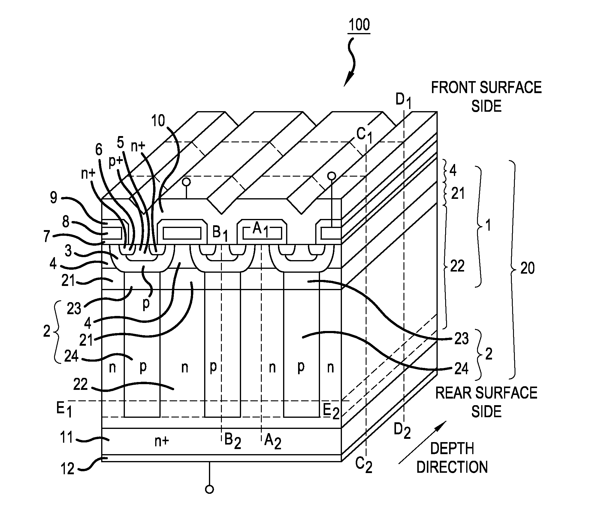
[0041]A super junction MOSFET will be described as an example of a super junction MOS semiconductor device according to Embodiment 1 of the invention. FIG. 1 is a perspective view illustrating the structure of the super junction MOSFET according to Embodiment 1 of the invention. As illustrated in FIG. 1, in a super junction MOSFET 100 according to Embodiment 1, a MOS gate (metal-oxide film-semiconductor insulated gate) structure is provided on the first main surface (front surface) side of a semiconductor substrate (an epitaxial substrate which will be described below) and an n+ drain layer 11 and a drain electrode 12 are provided on the second main surface (rear surface) side. The front surface structure of a planar MOSFET including the MOS gate structure includes, for example, a p base region 3, an n-type surface region 4, a p+ contact region 5, an n+ source region 6, a gate insulating film 7, a gate electrode 8, an interlayer insulating film 9, and a source electrode 10.

[0042]A p...

embodiment 2

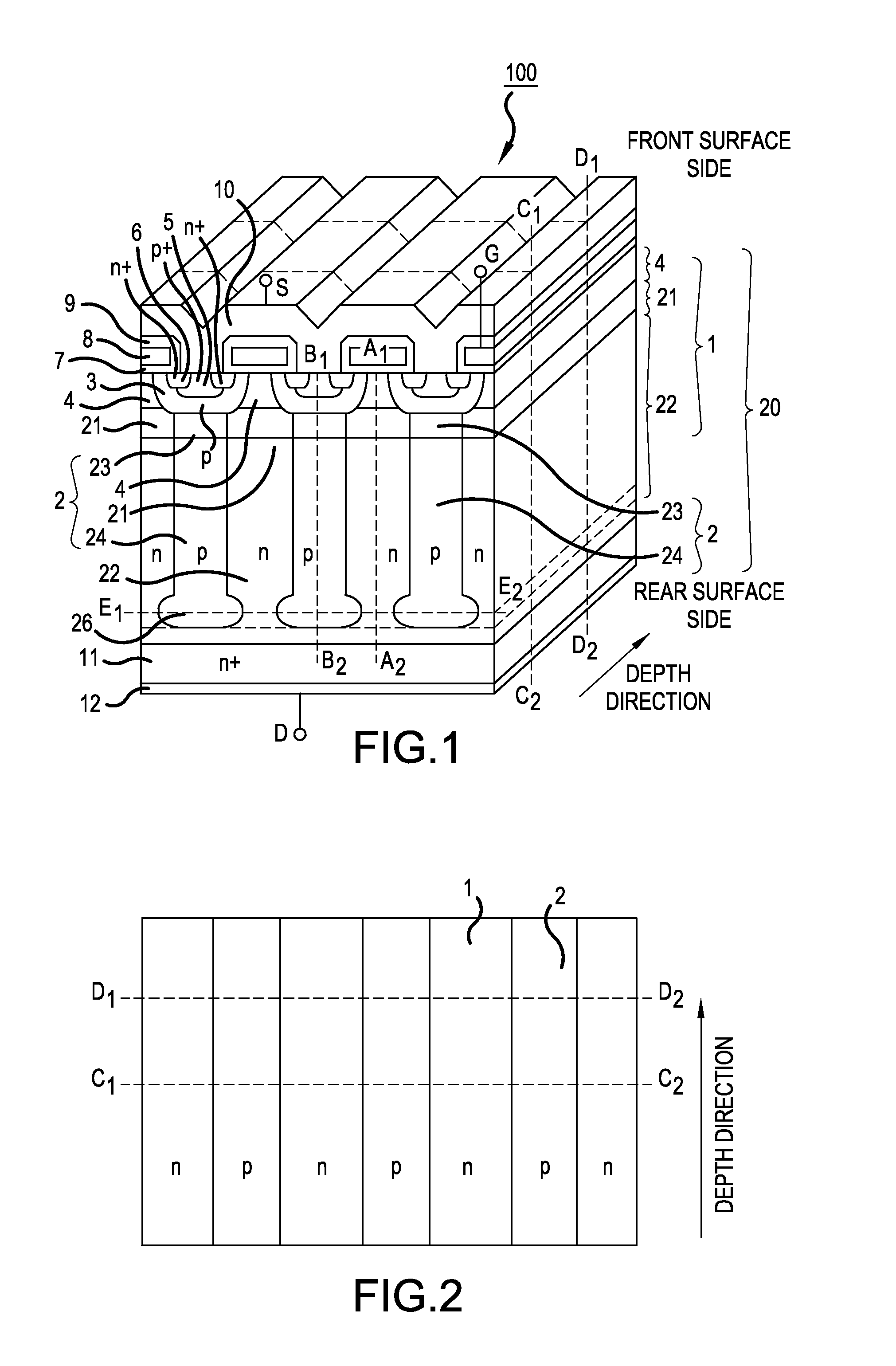
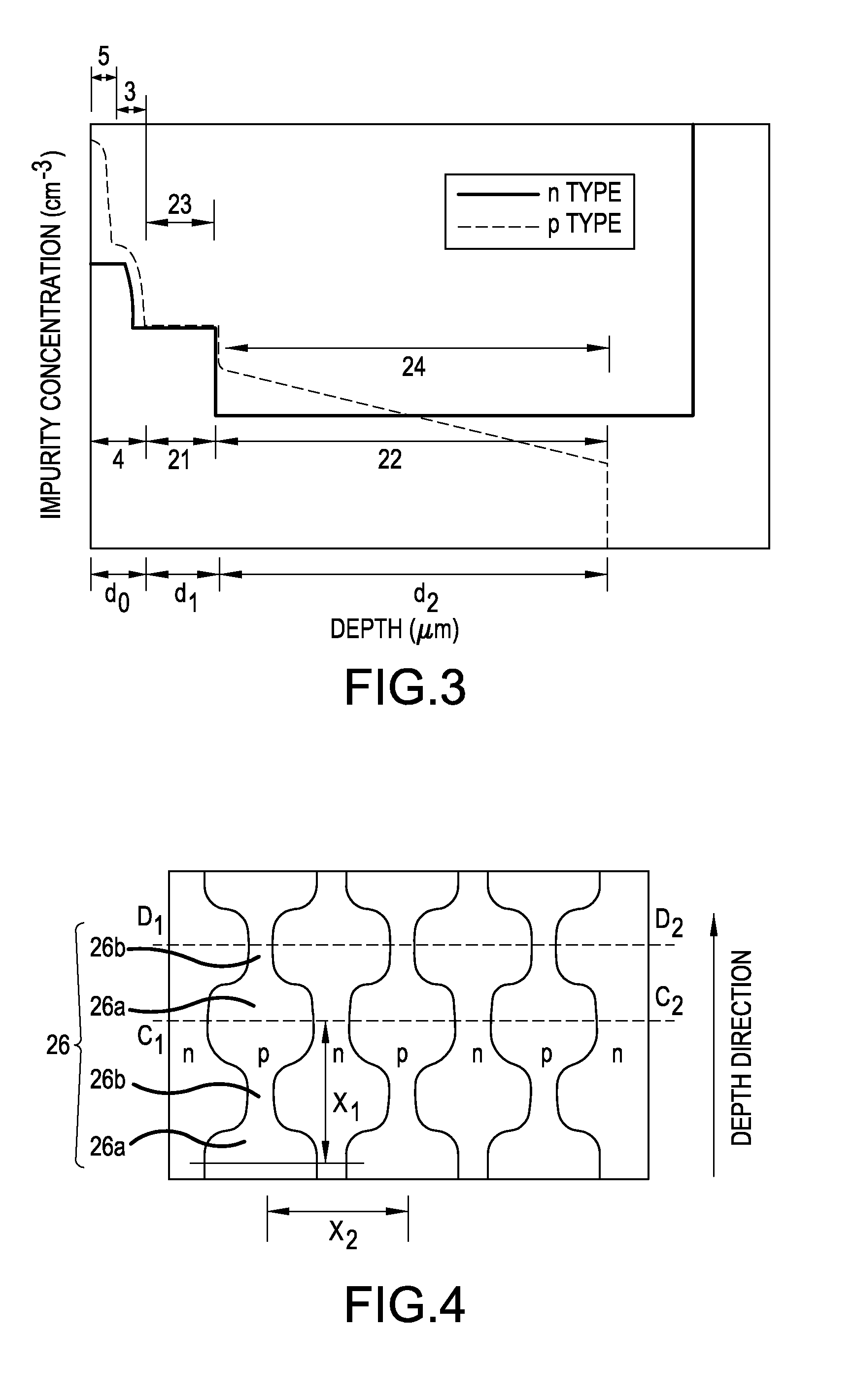
[0063]Next, a super junction MOSFET will be described as an example of a super junction MOS semiconductor device according to Embodiment 2 of the invention. FIG. 7 is a perspective view illustrating the structure of the super junction MOSFET according to Embodiment 2 of the invention. A parallel pn layer 20 of a super junction MOSFET 100 according to Embodiment 2 has a laminated structure of a plurality of epitaxial layers. In Embodiment 2, an n-type region 1 and a p-type region 2 forming the parallel pn layer 20 are formed as follows. Whenever an n-type epitaxial layer is grown, p-type impurity ions, such as boron ions, are implanted into the n-type epitaxial layer in order to form the p-type region 2 and the introduced p-type impurities are diffused to selectively form the p-type region 2 in the n-type epitaxial layer. A portion of the n-type epitaxial layer in which the p-type region 2 is not formed is the n-type region 1. For example, the parallel pn layer 20 having a pn junctio...


PUM


Abstract

An n− drift layer is a parallel pn layer having an n-type region and a p-type region are alternately arranged in the direction parallel to the main surface so as to come into contact with each other, and have a width in a direction parallel to the main surface of the substrate which is less than a length in a direction perpendicular to the main surface of the substrate. A second-main-surface-side lower end portion of the p-type region has a structure in which a high-concentration lower end portion and a low-concentration lower end portion of a p-type low-concentration region are repeated at a predetermined pitch in the direction parallel to the main surface of the substrate. It is possible to provide a super junction MOS semiconductor device which can improve a trade-off relationship between turn-off loss and turn-off dv / dt and improve avalanche resistance.

Description

BACKGROUND OF THE INVENTION[0001]A. Field of the Invention[0002]The present invention relates to a semiconductor device and a semiconductor device fabrication method.[0003]B. Description of the Related Art[0004]In a general planar n-channel vertical metal oxide semiconductor field effect transistor (MOSFET: insulated gate field effect transistor), among a plurality of semiconductor layers formed in a semiconductor substrate, an n− drift layer is a semiconductor layer with the highest resistance. When the thickness of the n− drift layer is reduced to shorten a current path, the resistance of the semiconductor layer with high resistance is reduced. Therefore, the overall on-resistance of the MOSFET is substantially reduced.[0005]However, in the off state of the MOSFET, a depletion layer spreads to the n− drift layer with high resistance and the breakdown voltage is maintained by the spreading of the depletion layer. Therefore, when the thickness of the n− drift layer is reduced, the s...

Claims


Application Information

Patent Timeline
Patent Type & Authority Applications(United States)
IPC IPC(8): H01L29/78H01L29/66H01L21/266H01L29/06H01L29/10
CPCH01L29/7802H01L29/0634H01L29/66712H01L21/266H01L29/1095H01L29/0696H01L29/0878H01L29/0886H01L29/36H01L29/66348H01L29/7395H01L29/7827
Inventor NIIMURA, YASUSHISAKATA, TOSHIAKI
Owner FUJI ELECTRIC CO LTD
Why Eureka
Try Eureka