Flexible display panel and manufacturing method thereof

a technology of flexible substrate and manufacturing method, applied in static indicating devices, instruments, non-linear optics, etc., can solve the problems of affecting the performance of devices, affecting the manufacturing yield, and affecting the peeling issue between the flexible substrate and the signal transmission circuit, so as to achieve convenient manufacturing and avoid peeling. , the effect of convenient reliability

Active Publication Date: 2014-12-25
AU OPTRONICS CORP
View PDF2 Cites 21 Cited by
  • Summary
  • Abstract
  • Description
  • Claims
  • Application Information

AI Technical Summary

Benefits of technology

[0025]To recapitulate, in the embodiments of the disclosure, the processes of manufacturing the active element, the display device and the pad on the carrier substrate (such as the glass substrate) are not restricted by the process temperature of the flexible substrate. Additionally, since the flexible display panel is connected to the signal transmission circuit after releasing from the carrier substrate during the manufacturing process thereof; the issue related to the signal transmission circuit peeling from the flexible display panel can be prevented while releasing, such that the flexible display panel has a preferable reliability. Moreover, in the disclosure, the pad is exposed after releasing from the carrier substrate, which can be connected to the signal transmission circuit directly in the manufacturing method of the flexible display panel. Thus, the manufacturing method of the flexible display panel has a relatively simplified manufacturing procedure.

Problems solved by technology

Since the flexible substrate is directly fabricated on the rigid substrate, the circumstances such disconnection or crack are likely to occur due to stress while releasing from the rigid substrate, thereby causing the manufacturing yield to decrease.
Furthermore, when the flexible substrate is a plastic substrate, the fabrication of active element and display device on the flexible substrate are easy to be restricted by the process temperature of the plastic substrate, such that the performance of the device is affected.
If the release between the flexible substrate and the rigid substrate is performed after the flexible substrate is connected with the signal transmission circuit, the peeling issue between the flexible substrate and the signal transmission circuit is likely to occur.
By this way, besides the manufacturing steps become rather complicated, the manufacturing yield is also easily affected when the protective film is adhered and torn off repeatedly.

Method used


Image

  • Flexible display panel and manufacturing method thereof
  • Flexible display panel and manufacturing method thereof
  • Flexible display panel and manufacturing method thereof

Examples


first embodiment

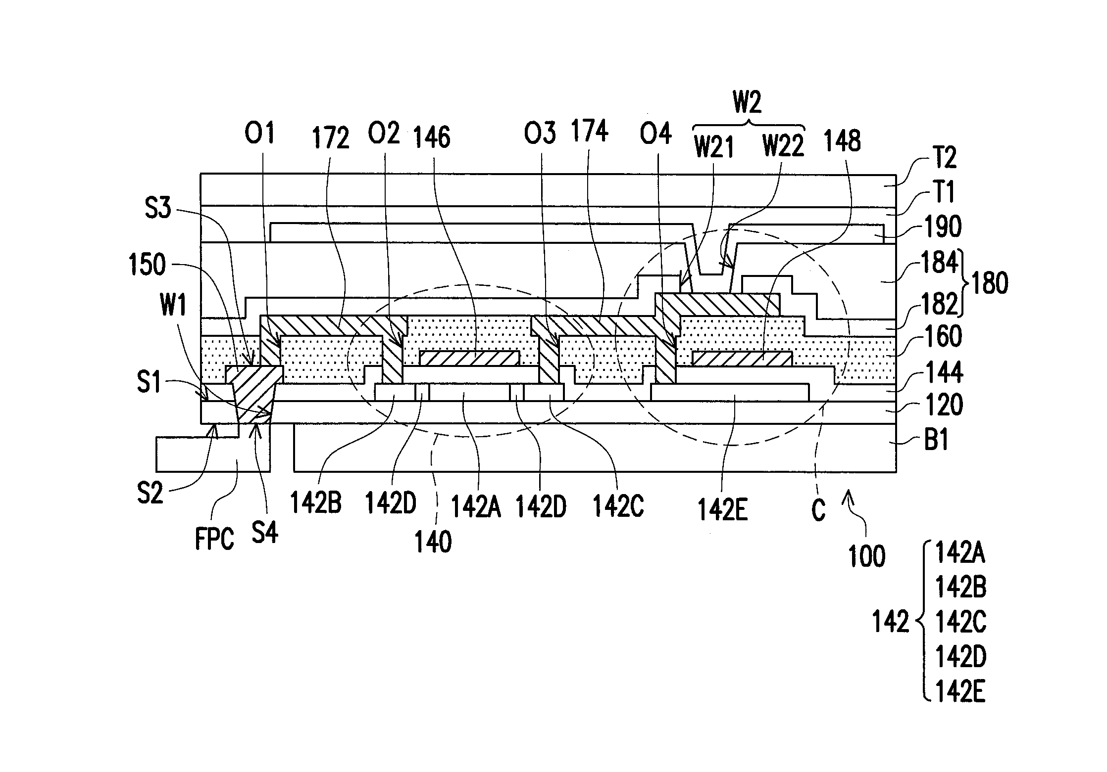
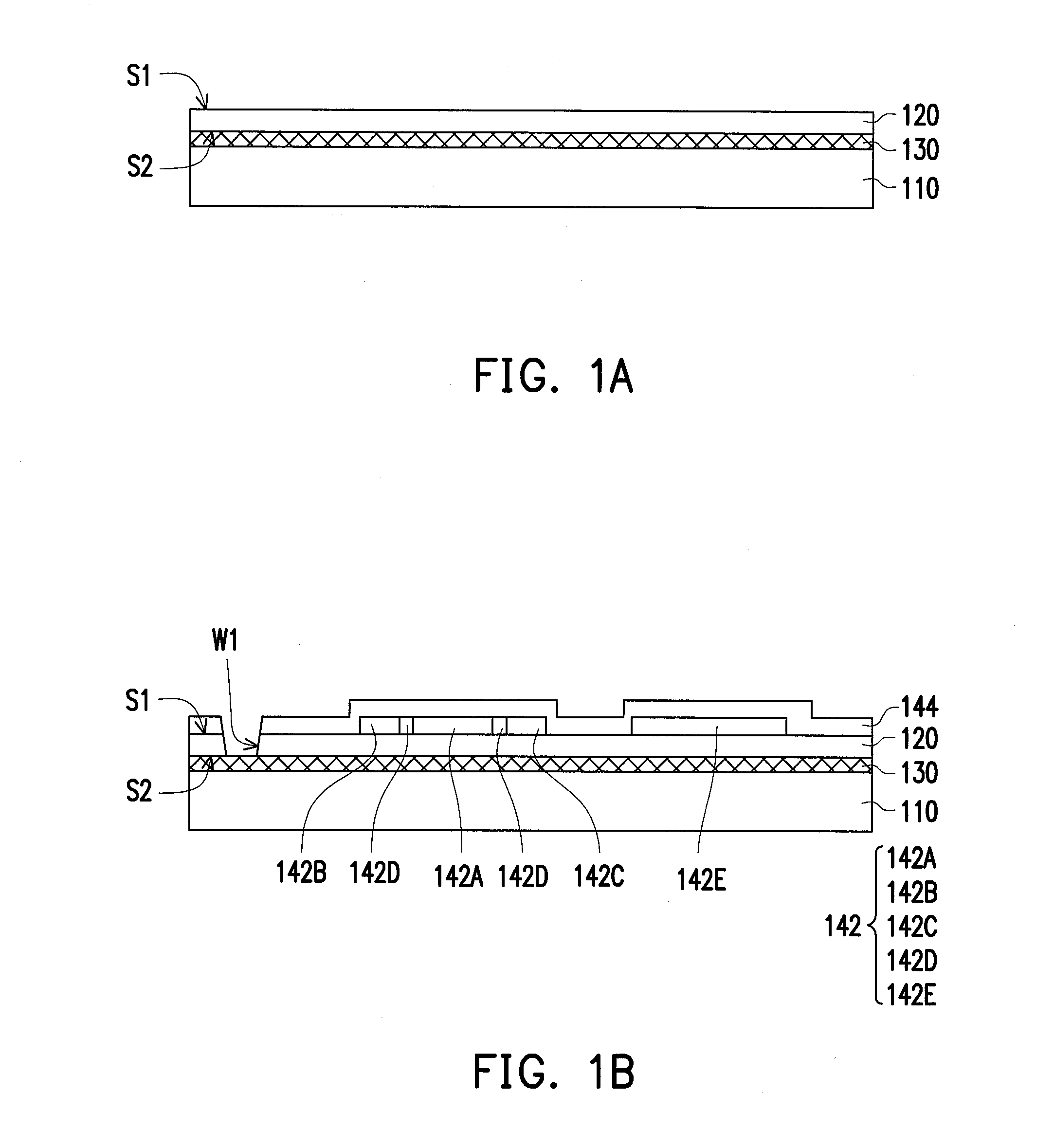
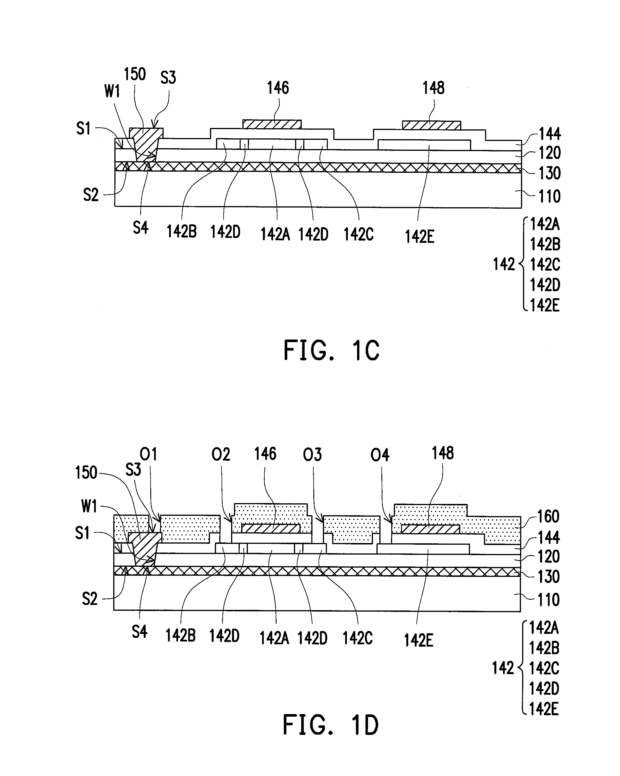
[0030]FIG. 1A through FIG. 1I are schematic diagrams illustrating a manufacturing process of a flexible display panel in a cross-sectional view according to a first embodiment of the disclosure. Referring to FIG. 1A, a buffer layer 120 is formed on the carrier substrate 110. The buffer layer 120 has a first surface S1 and a second surface S2 opposite to the first surface S1, in which the second surface S2 is located between the first surface S1 and the carrier substrate 110, for instance. In the embodiment, the carrier substrate 110 can be configured to be a carrier for carrying the subsequent manufactured devices. For example, the material of the carrier 110 can be glass, quartz, polyester, polycarbonate or other materials with a certain rigidity. On the other hand, the buffer layer 120 can be configured to block the impurities contained in the carrier substrate 110 to diffuse. For example, the material of the buffer layer 120 can be silicon oxide or silicon nitride with high diele...

second embodiment

[0051]FIG. 2A through FIG. 21 are schematic diagrams illustrating a manufacturing process of a flexible display panel in a cross-sectional view according to a second embodiment of the disclosure. It should be noted that portions of the detailed implementation of manufacturing processes in the following embodiment are similar to those disclosed by the afore-described embodiment, so that the detailed description may be referred to the descriptions above, which is not repeated therein. The difference between the first embodiment and the second embodiment is the structure of the pad 150A, the gate 146A and the upper electrode 148A depicted in FIG. 2C and the manufacturing method thereof.

[0052]Referring to FIG. 2C, the pad 150A, the gate 146A and the upper electrode 148A in the embodiment are respectively formed by stacking the first conductive layer and the second conductive layer together. For instance, the formation thereof is to sequentially form the first conductive layer and the se...


PUM

PropertyMeasurementUnit
conductiveaaaaaaaaaa
flexibleaaaaaaaaaa
flexibilityaaaaaaaaaa

Abstract

A flexible display panel including a buffer layer, an active element, a pad, a display device and a signal transmission circuit is provided. The active element is located on the buffer layer. The pad is located in the buffer layer and is electrically connected to the active element. The display device is located on the active element and is electrically connected to the active element, in which the display device includes a pixel electrode, an opposite electrode and a display medium layer located therebetween. The active element and the signal transmission circuit are respectively located at a first surface and a second surface of the buffer layer, the second surface is opposite to the first surface, and the signal transmission circuit is electrically connected to the active element via the pad. A manufacturing method of a flexible display panel is also provided.

Description

CROSS-REFERENCE TO RELATED APPLICATION[0001]This application claims the priority benefit of Taiwan application serial no. 102122587, filed on Jun. 25, 2013. The entirety of the above-mentioned patent application is hereby incorporated by reference herein and made a part of this specification.BACKGROUND[0002]1. Field of the Invention[0003]The disclosure relates to a display panel and a manufacturing method thereof, and more particularly, to a flexible display panel and a manufacturing method thereof.[0004]2. Description of Related Art[0005]With rapid development of display technologies, conventional cathode ray tube (CRT) displays have been gradually replaced by flat panel displays (FPD). In comparison with the FPD formed by a rigid substrate (e.g. a glass substrate), a flexibly display in which an active element is formed on a flexible substrate has been developed according to recent researches because the flexible substrate (e.g. a plastic substrate) is characterized by flexibility...

Claims


Application Information

Patent Timeline
Patent Type & Authority Applications(United States)
IPC IPC(8): G02F1/1333H01L27/32G02F1/133
CPCG02F1/133305H01L27/32G02F1/13306G02F1/1345G02F1/136286H01L27/1266H01L29/78603H01L27/1218H01L27/124H10K59/131H10K71/80H10K59/1201H10K2102/311
Inventor CHEN, YUNG-PEIFANG, CHUN-HSIANGTSAI, CHIH-HUNG
Owner AU OPTRONICS CORP
Why Eureka
Try Eureka