Organic light emitting diode display device

a light-emitting diode and display device technology, applied in the direction of thermoelectric device junction materials, semiconductor devices, electrical apparatus, etc., can solve the problems of poor interface characteristics between ground lines b>, inability to form strong bonds with adjacent materials, poor bond between these two layers, etc., to prevent the generation of blotches, high display quality, and high reliability

Active Publication Date: 2015-01-01
LG DISPLAY CO LTD
View PDF53 Cites 15 Cited by
  • Summary
  • Abstract
  • Description
  • Claims
  • Application Information

AI Technical Summary

Benefits of technology

[0015]An aspect of this document is to provide an organic light emitting diode display device which offers high display quality and high reliability by preventing the generation of blotches in a display region and blocking the path through which moisture from the outside permeates into a light emitting layer.
[0016]To achieve the above advantages, one exemplary embodiment provides an organic light emitting diode display device comprising: a substrate comprising a display region and a non-display region; a thin film transistor formed in the display region; an organic light emitting layer connected to the thin film transistor; a bank formed to define a light emitting region of the organic light emitting layer; a metal pattern disposed in the non-display region and not covered with the bank; a first conductive pattern connected to the organic light emitting layer that is also connected to the metal pattern; and a second conductive pattern connected to the metal pattern that is physically separated from the first conductive pattern. According to this aspect, the organic light emitting diode display device solves the problem of degradation in adhesion force caused by the initial deposition and removal of the bank layer on the metal pattern, as the first and second conductive patterns are formed prior to the bank layer.
[0018]The first metal pattern and the second metal pattern are electrically connected to each other. According to this aspect, the ground line may be connected in parallel so that conductivity enhancement and a decrease in the width of the ground line formed per unit area can be achieved, contributing to reducing the bezel.
[0019]According to this aspect, the first and second conductive patterns function to prevent moisture or oxide components from permeating into the organic light emitting layer. In the case of moisture permeation through the first conductive pattern from the outside, the separation between the first and second conductive patterns prevents the moisture from further permeating into the second conductive pattern.

Problems solved by technology

However, a problem arises from depositing and then removing / patterning the bank layer 160 in this way.
Poor interface characteristics include the inability to form a strong bond with adjacent materials.
As a result, when the bank layer 160 is initially formed and then removed from the ground line 70, leftover bank layer that was not able to be removed during the removal process will result in poor interface characteristics between the ground line 70 and whatever layer is later formed on the ground line 70.
Consequently, the leftover bank layer in between the ground line 70 and the cathode can result in a poor bond between these two layers.
As a result, the two layers may separate over time, and create a path for moisture to penetrate into the display region of the device.
Over time, this may negatively affect the performance of the organic light emitting diode display device.
The leftover bank layer may also create visible blotches in the display region, which is highly undesirable.

Method used


Image

  • Organic light emitting diode display device
  • Organic light emitting diode display device
  • Organic light emitting diode display device

Examples


Embodiment Construction

[0031]Reference will now be made in detail to embodiments of the invention, examples of which are illustrated in the accompanying drawings. Wherever possible, the same reference numbers will be used throughout the drawings to refer to the same or like parts. It will be paid attention that detailed description of known arts will be omitted if it is determined that the arts can mislead the embodiments of the invention.

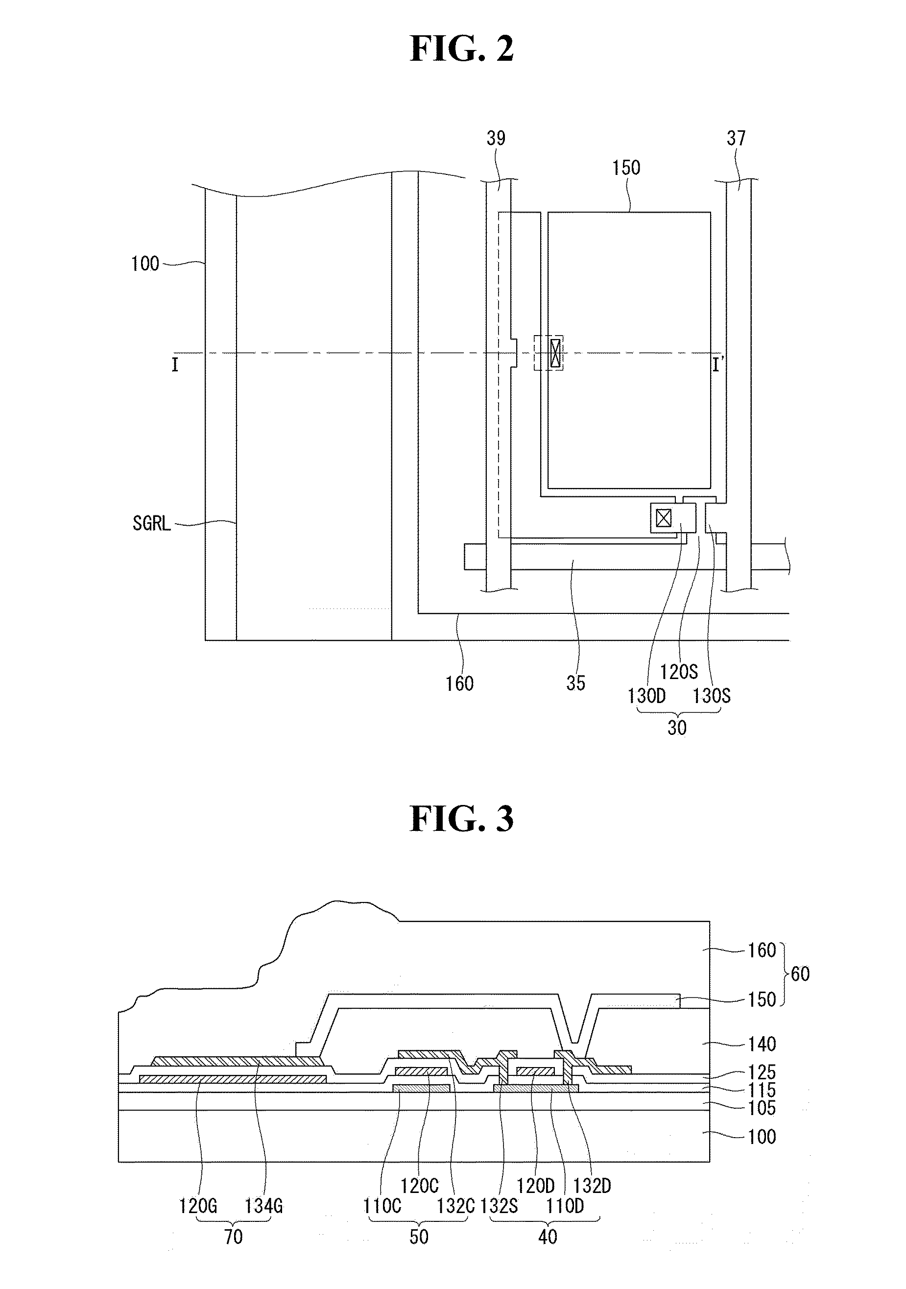
[0032]Hereinafter, an organic light emitting diode display device according to an exemplary embodiment will be described with reference to FIGS. 5 to 7b. FIG. 5 is a top plan view showing the structure of an organic light emitting diode display device using a thin film transistor as an active element according to the present invention. FIG. 6 is a cross-sectional view taken along the line II-II′ of FIG. 5. FIGS. 7a and 7b are photographs showing APC corrosion of a conductive pattern.

[0033]Referring to FIGS. 5 and 6, the organic light emitting diode display according to t...


PUM


Abstract

The present invention provides an organic light emitting diode display device comprising a substrate comprising a display region and a non-display region, a thin film transistor formed in the display region; an organic light emitting layer connected to the thin film transistor, a bank formed to define a light emitting region of the organic light emitting layer, a metal pattern disposed in the non-display region and not covered with the bank; and a conductive pattern connected to the organic light emitting layer while covering the metal pattern and partially physically separated on the metal pattern.

Description

[0001]This application claims the priority benefit of Korea Patent Application No. 10-2013-0073556 filed on Jun. 26, 2013, which is incorporated herein by reference for all purposes as if fully set forth herein.BACKGROUND[0002]1. Field of the Art[0003]This document relates to an organic light emitting diode display device, and more particularly, to an organic light emitting diode display device which has a structure devised to overcome defects that might occur during the process of simplifying the manufacture of the organic light emitting diode display device.[0004]2. Discussion of the Related Art[0005]In recent years, various types of flat panel displays having reduced weight and volume, which are drawbacks of cathode ray tubes (CTRs), have been developed. These flat panel displays comprise liquid crystal displays (LCDs), field emission displays (FEDs), plasma display panels (PDPs), and electroluminescence devices (ELs).[0006]FIG. 1 is a top plan view showing the structure of an or...

Claims


Application Information

Patent Timeline
Patent Type & Authority Applications(United States)
IPC IPC(8): H01L27/32H01L51/52
CPCH01L51/52H01L27/3244H01L27/3276H01L51/5246H10K59/131H10K50/8426H10K50/844H10K59/87H10K59/10H10K59/122H10K59/12H10K50/00H10K50/80H10K50/84
Inventor SUNG, KIYOUNGKIM, SANGSOOSHIN, SANG-IL
Owner LG DISPLAY CO LTD
Why Eureka
Try Eureka