OLED Panel and Package Method Thereof

a technology of oled panel and package method, which is applied in the manufacture of electrode systems, electric discharge tube/lamps, and discharge tube luminescnet screens, etc., can solve the problems of large packaging requirements, large gap, and significant decay of brightness and life time, and achieves less residual water and oxygen, small sealing space, and simple structure

Inactive Publication Date: 2015-01-08
TCL CHINA STAR OPTOELECTRONICS TECH CO LTD
View PDF7 Cites 12 Cited by
  • Summary
  • Abstract
  • Description
  • Claims
  • Application Information

AI Technical Summary

Benefits of technology

[0008]The object of the present invention is to provide an OLED panel, which has simple structure, smaller sealing space, less residual water and oxygen, and longer lifetime.

Problems solved by technology

However, the organic materials are sensitive to water vapor and oxygen, which is susceptible to degeneration and aging due to water and oxygen, so that the brightness and life time will significantly decay.
Therefore, as a display device based on organic materials, the demands of the package of the OLED device are very heavy.
However, the OLED panel formed in this way has a certain gap between the OLED package cover and the OLED substrate.
The existence of the gap increases the existing possibility of residual water and oxygen, which affects the lifetime of the OLED panel.
However, the OLED panel obtained by the sealing method still has larger gap between the first and second glass substrates 100, 400, which increases the possibility of residual water and oxygen existing in the sealing body and affects the lifetime of the OLED panel.

Method used


Image

  • OLED Panel and Package Method Thereof
  • OLED Panel and Package Method Thereof
  • OLED Panel and Package Method Thereof

Examples


Embodiment Construction

[0031]In order to more clearly describe the technical solutions and the effects in the present invention, the preferred embodiment of the present invention accompanying drawings are described in detail as follows.

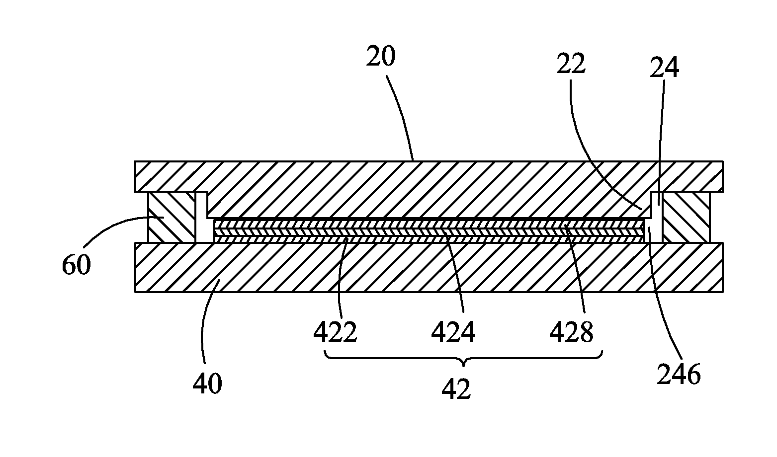
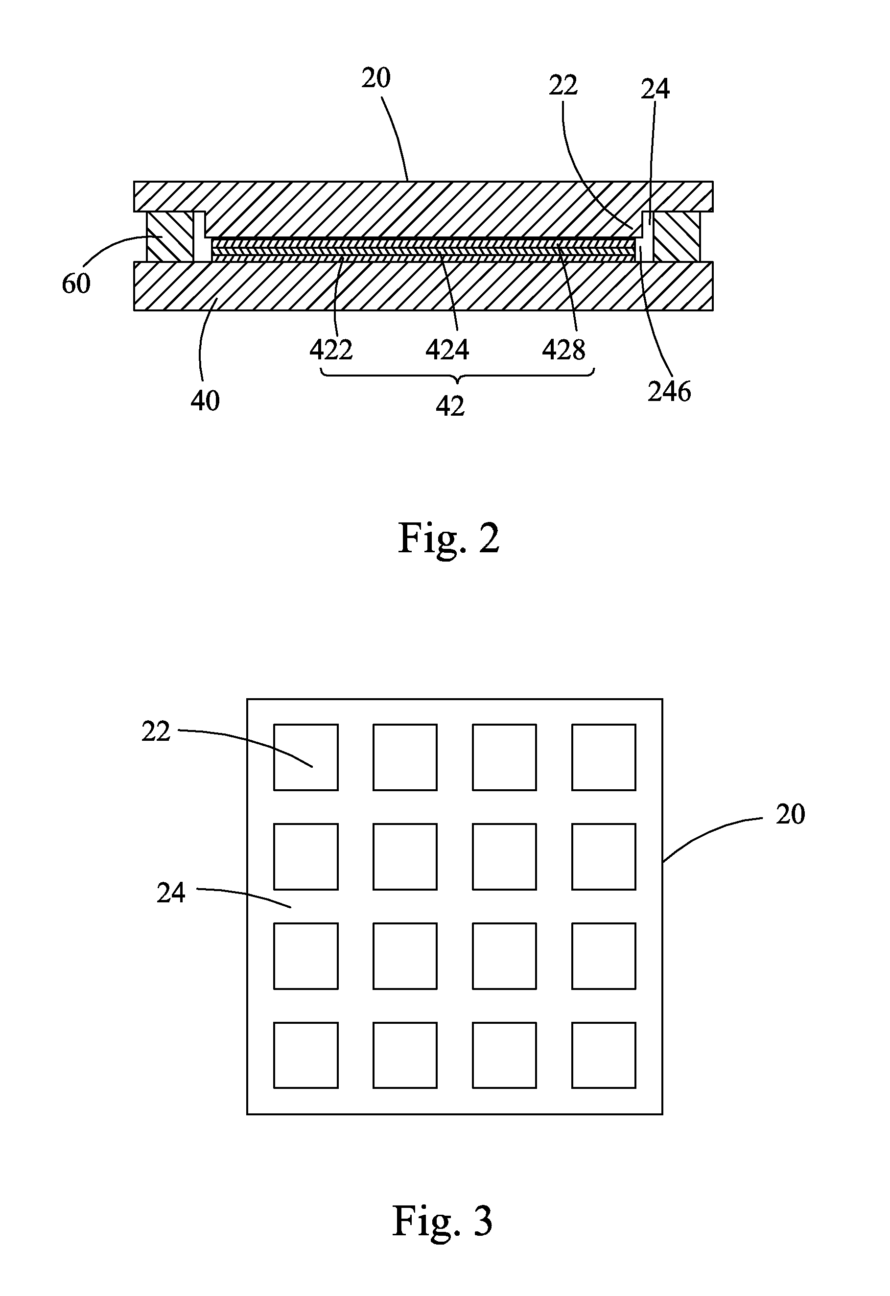
[0032]Referring to FIGS. 2 and 5, the present invention provides an OLED panel, comprising: a substrate 40, multiple OLED devices 42 formed on the substrate 40, a package cover 20 attached oppositely to the substrate 40 and multiple sealed plastic frame 60 provided between the substrate 40 and the package cover 20 and corresponding to the OLED device 42. The package cover 20 is provided with multiple protrusions 22 corresponding to the multiple OLED devices 42. A groove 24 is formed around the protrusion 22. The sealed plastic frame 60 is located in the groove 24. The lower surface of the protrusion 22 is close to the upper surface of the OLED device 42, so that a sealing space 246 formed within the package cover 20, the substrate 40 and the sealed plastic frame 60 is small...


PUM


Abstract

The present invention provides an OLED panel and the package method thereof. The OLED panel comprises: a substrate 40, multiple OLED devices 42 formed on the substrate 40, a package cover 20 attached oppositely to the substrate 40 and multiple sealed plastic frame 60 provided between the substrate 40 and the package cover 20 and corresponding to the OLED device 42. The package cover 20 is provided with multiple protrusions 42 corresponding to the multiple OLED devices 22. A groove 24 is formed around the protrusion 22. The sealed plastic frame 60 is located in the groove 24. The lower surface of the protrusion 22 is close to the upper surface of the OLED device 42.

Description

BACKGROUND OF THE INVENTION[0001]1. Field of the Invention[0002]The present invention relates to the field of flat panel display techniques, and in particular to an OLED panel and the package method thereof.[0003]2. The Related Arts[0004]Flat display device has many advantages of thin body, low power, no radiation, etc., so it has been widely applied. The flat display device according to the prior art mainly comprises liquid crystal display (LCD) and organic light emitting display (OLED).[0005]The organic light emitting display device has characteristics of self-luminous, high brightness, wide viewing angle, high contrast, flexible, low power consumption, etc. So, it has been widely concerned and is a new generation of display, which has begun to gradually replace the traditional liquid crystal display device and is widely used in mobile phone screen, computer monitor, full-color television and other electronic products. OLED display technology differs from traditional LCD display, ...

Claims


Application Information

Patent Timeline
Patent Type & Authority Applications(United States)
IPC IPC(8): H05B33/04H05B33/10
CPCH05B33/10H05B33/04H10K50/841H10K50/8426
Inventor YU, WEI
Owner TCL CHINA STAR OPTOELECTRONICS TECH CO LTD
Why Eureka
Try Eureka