Wafer processing chamber and method for transferring wafer in the same

a technology of processing chamber and transferring chamber, which is applied in the directions of pile separation, transportation and packaging, article separation, etc., can solve the problems of non-uniformity of the wafer, considerable problem of polymer accumulation in the pin hole, and common arcing, so as to improve the electrical properties of the device fabricated, the effect of effectively preventing the arcing issu

Inactive Publication Date: 2015-01-08
UNITED MICROELECTRONICS CORP
View PDF8 Cites 335 Cited by
  • Summary
  • Abstract
  • Description
  • Claims
  • Application Information

AI Technical Summary

Benefits of technology

[0010]The disclosure is directed to a wafer processing chamber and a method for transferring wafer in the same. In the embodiment, a wafer processing chamber with improved electrostatic chuck is provided, and the arcing issue could be effectively prevented in the wafer processing procedures, thereby improving the electrical properties of the device fabricated on the wafer of the embodiment.

Problems solved by technology

Arcing is a common problem in the plasma processing systems for various reasons.
The arcing defects have considerable effects on various process parameters, such as the deposition and / or etch rates, thereby causing non-uniformities on the wafer.
A known method has been proposed by enlarging the pin hole, but this would cause another considerable issue of polymer accumulation in the pin hole during wafer processing.

Method used


Image

  • Wafer processing chamber and method for transferring wafer in the same
  • Wafer processing chamber and method for transferring wafer in the same
  • Wafer processing chamber and method for transferring wafer in the same

Examples


first embodiment

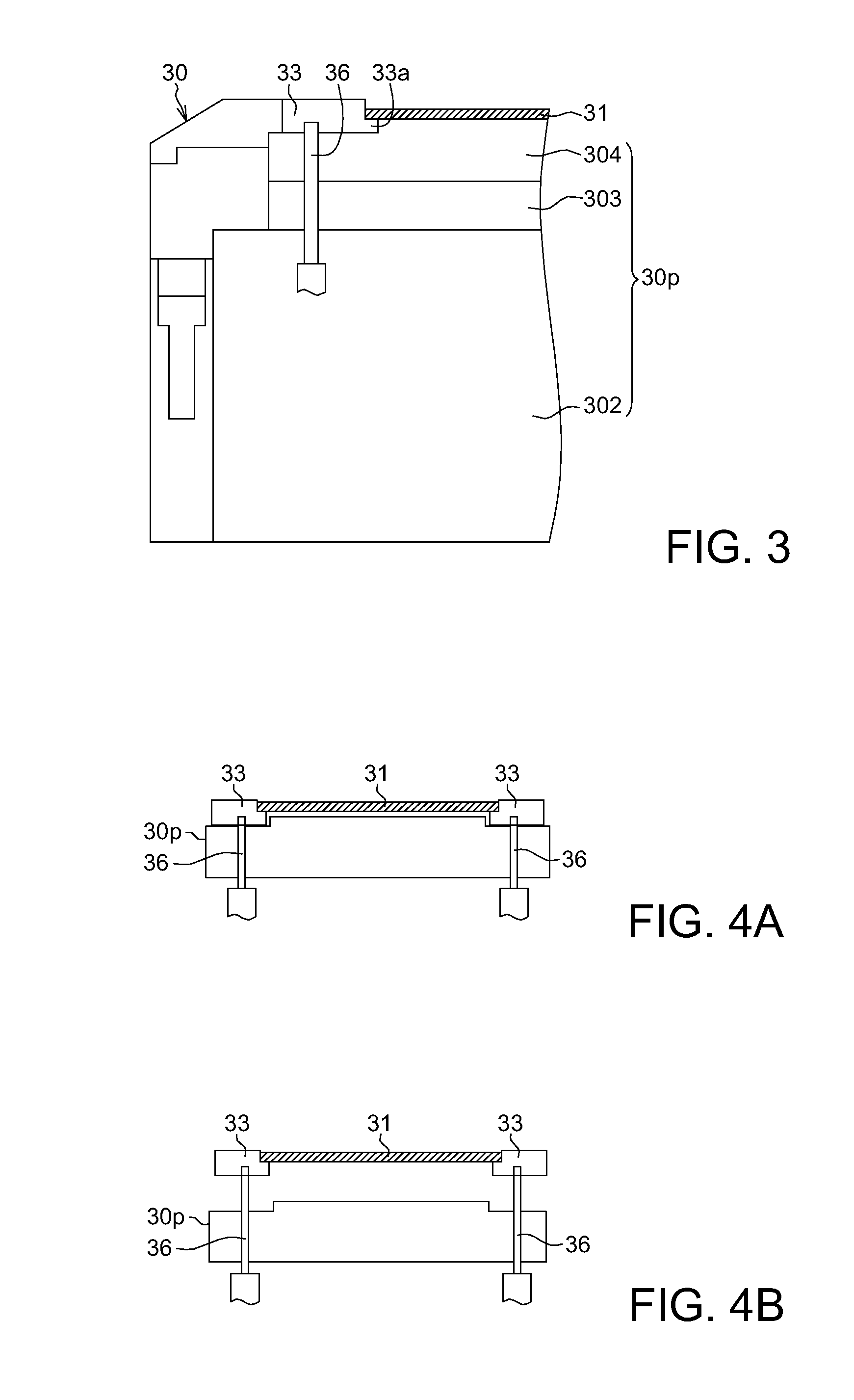
[0026]FIG. 3 is a schematic diagram illustrating part of a configuration of a wafer positioned on an electrostatic chuck of a wafer processing chamber according to the present disclosure. A wafer processing chamber has an electrostatic chuck 30 which at least comprises a processing platform 30p, a focus ring 33 disposed above the processing platform 30p for setting a wafer 31, and a lifting apparatus 36 coupled to the processing platform 30p and positioned corresponding to the focus ring 33. The focus ring 33 is moved by the lifting apparatus 36 for lifting the wafer 31 and the focus ring 33 up and down together.

[0027]In one embodiment, the processing platform 30p comprises a conductive plate 302, an electrode 303 and an insulating layer 304, wherein the electrode 303 is disposed between the conductive plate 302 and the insulating layer 304, and embedded in the insulating layer 304. The wafer 31 is loaded on a focus ring 33 above the insulating layer 304. A DC voltage from a DC powe...

second embodiment

[0035]FIG. 6 is a schematic diagram illustrating part of a configuration of a wafer positioned on an electrostatic chuck of a wafer processing chamber according to the present disclosure. A wafer processing chamber has an electrostatic chuck 50 which at least comprises a processing platform 50p, a focus ring 53 disposed above the processing platform 50p for setting a wafer 51, and a lifting apparatus 56 coupled to the processing platform 50p and positioned corresponding to the focus ring 53. The focus ring 53 is moved by the lifting apparatus 56 for lifting the wafer 51 and the focus ring 53 up and down together.

[0036]In the second embodiment, the lifting apparatus 56 comprises a first magnetic unit 563 and a second magnetic unit 565. The first magnetic unit 563 is disposed above the focus ring 53, and the second magnetic unit 565 is disposed on the upper surface of the focus ring 53. Also, wafer loading and / or unloading procedures are not disturbed by the positions of the first mag...

third embodiment

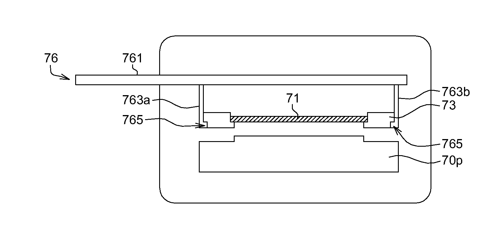
[0042]Similarly, a wafer processing chamber has an electrostatic chuck which at least comprises a processing platform 70p, a focus ring 73 disposed above the processing platform 70p for setting a wafer 71. The lifting apparatus 76 of the third embodiment is coupled to the processing platform 70p and positioned above to the focus ring 73. The focus ring 73 is moved by the lifting apparatus 76 for lifting the wafer 71 and the focus ring 73 up and down together. Also, the wafer loading and / or unloading procedures are not disturbed by the positions of the lifting apparatus 76.

[0043]Please refer to FIG. 8A˜FIG. 8C, FIG. 9A and FIG. 9B together. The lifting apparatus 76 of the third embodiment comprises a cantilever beam 761 and three clutch arms 763a, 763b and 763c connected to the cantilever beam 761. As shown in FIG. 8A˜FIG. 8C, each end of the clutch arms 763a, 763b and 763c includes a protrusion 765 (projected from the clutch arms 763a, 763b and 763c and towards the focus ring 73). I...


PUM

PropertyMeasurementUnit
magneticaaaaaaaaaa
magnetic fieldaaaaaaaaaa
polaritiesaaaaaaaaaa

Abstract

A wafer processing chamber and a method for transferring wafer in the same are provided to prevent the arcing issue. In the embodiments, a wafer is positioned on the focus ring, and a lifting apparatus is provided outside the wafer such as corresponding to the focus ring. The lifting apparatus of the embodiment could be positioned below or above the focus ring. The wafer and the focus ring are lifted together by the lifting apparatus, and transferred together by a transferring unit.

Description

BACKGROUND[0001]1. Technical Field[0002]The disclosure relates in general to a wafer processing chamber and a method for transferring wafer in the same, and more particularly to the wafer processing chamber to prevent the arcing issue in the plasma processing procedures.[0003]2. Description of the Related Art[0004]In the semiconductor fabrication, wafer is generally fixed at an electrostatic chuck, and a plasmas chamber is utilized for depositing a material on or etching the wafer. FIG. 1 is a schematic diagram illustrating part of a configuration of a wafer positioned on an electrostatic chuck of a conventional wafer processing chamber. In the conventional wafer processing chamber, a wafer 11 is positioned on a mounting table of an electrostatic chuck 10, the mounting table comprises a conductive plate 102, an electrode 103 on the conductive plate 102 and an insulating layer 104. The electrode 103 is disposed between the conductive plate 102 and the insulating layer 104, and embedd...

Claims


Application Information

Patent Timeline
Patent Type & Authority Applications(United States)
IPC IPC(8): H01L21/677H01J37/32
CPCH01J37/32715H01L21/67745H01J37/32743H01L21/67748H01L21/68707H01L21/68742
Inventor CAI, YAN
Owner UNITED MICROELECTRONICS CORP
Why Eureka
Try Eureka