Thin film transistor, and thin film transistor array panel and organic light emitting diode display including the same

a thin film transistor and array panel technology, applied in transistors, thermoelectric devices, solid-state devices, etc., can solve the problems of overlying layer contact defect generation and underlying layer contact defect generation, and achieve the effect of reducing contact defect generation and increasing the alignment margin of the mask

Active Publication Date: 2015-01-15
SAMSUNG DISPLAY CO LTD
View PDF4 Cites 9 Cited by
  • Summary
  • Abstract
  • Description
  • Claims
  • Application Information

AI Technical Summary

Benefits of technology

[0029]As shown in the exemplary embodiment, when defining the contact hole, the alignment margin of the mask is increased such that the generation of the contact defect may be reduced.

Problems solved by technology

When the misalignment is generated, underlying semiconductor or metal layers are not exposed through the contact holes such that a contact defect of overlying layers and underlying layers may be generated.

Method used


Image

  • Thin film transistor, and thin film transistor array panel and organic light emitting diode display including the same
  • Thin film transistor, and thin film transistor array panel and organic light emitting diode display including the same
  • Thin film transistor, and thin film transistor array panel and organic light emitting diode display including the same

Examples


Embodiment Construction

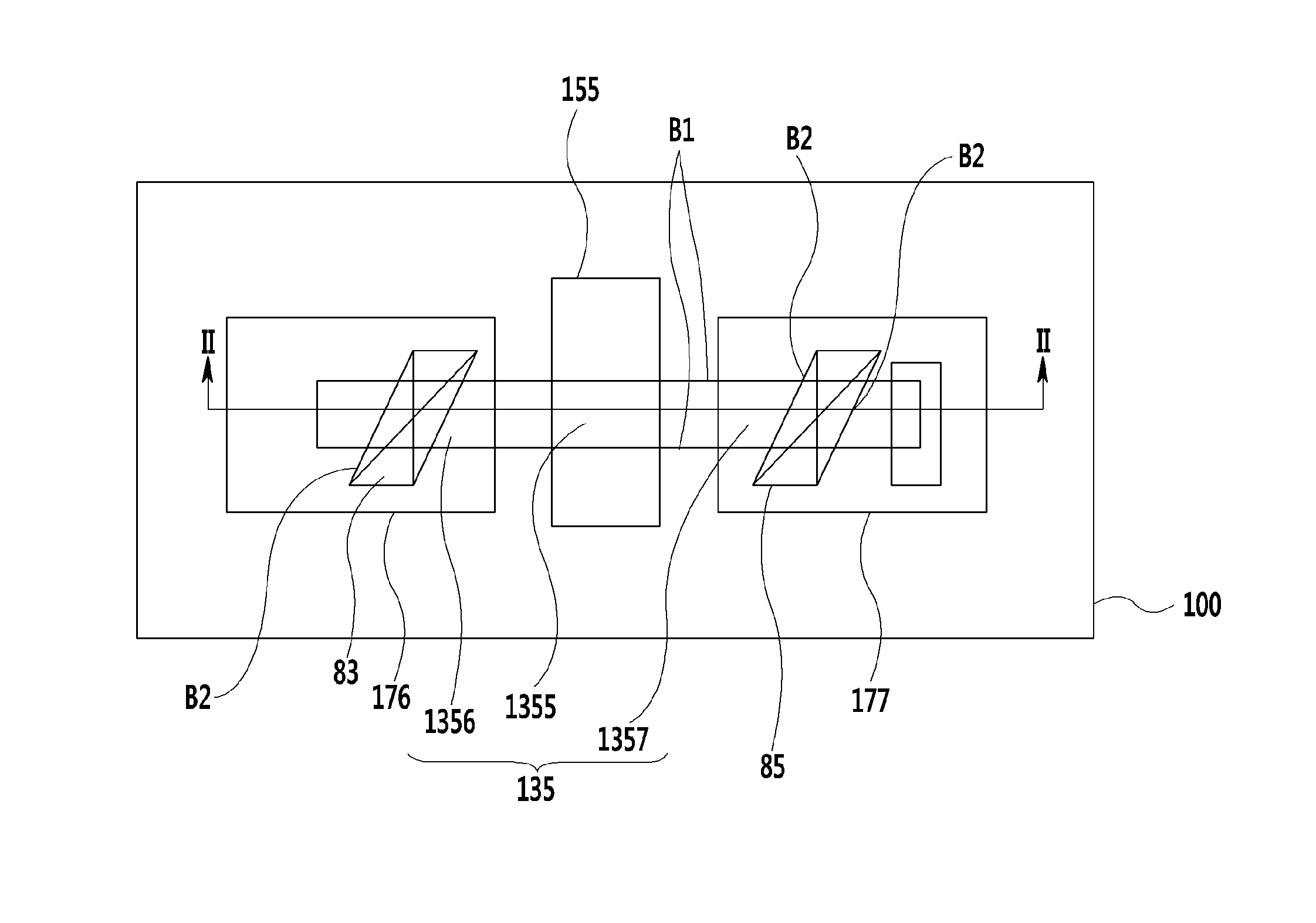
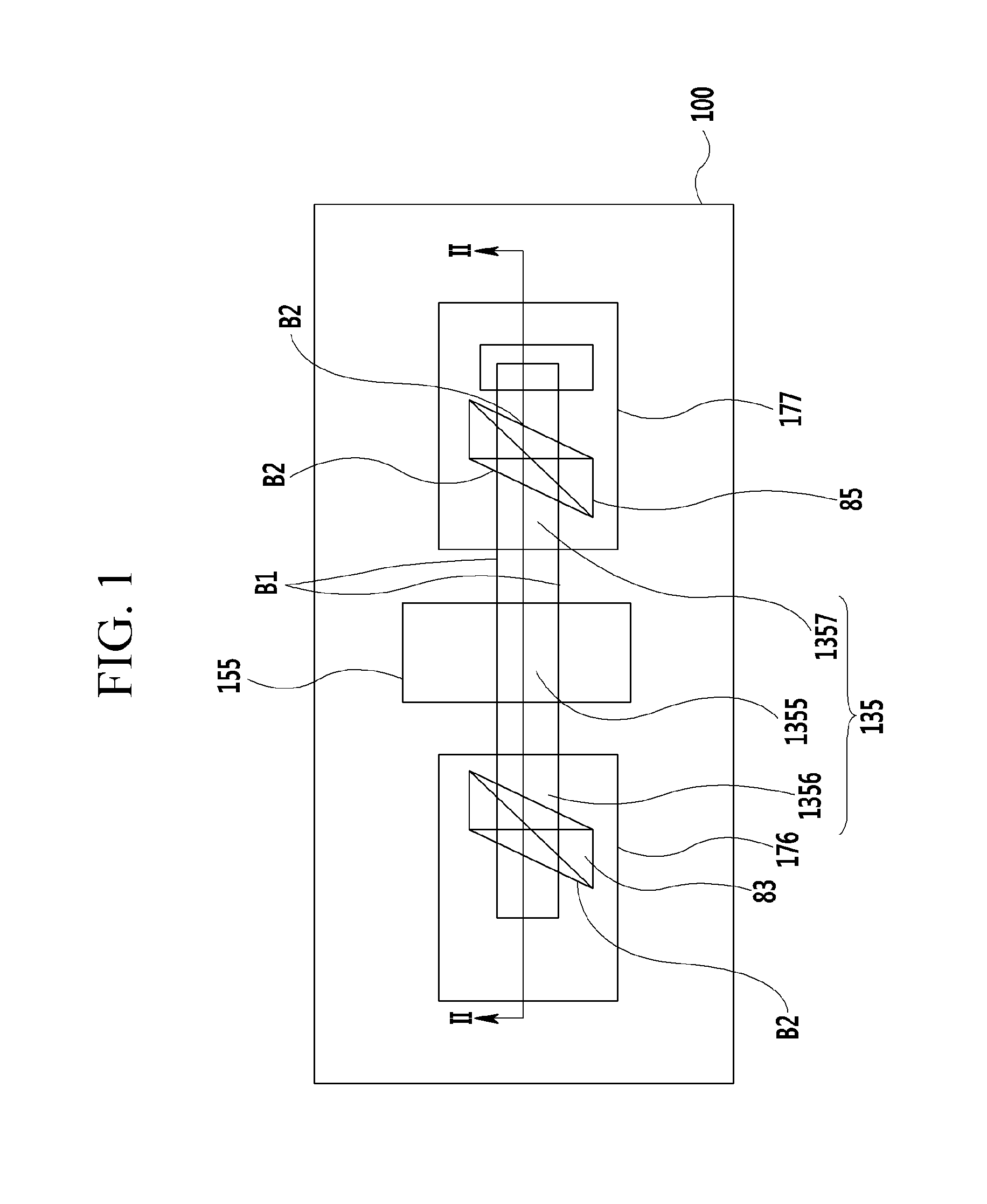
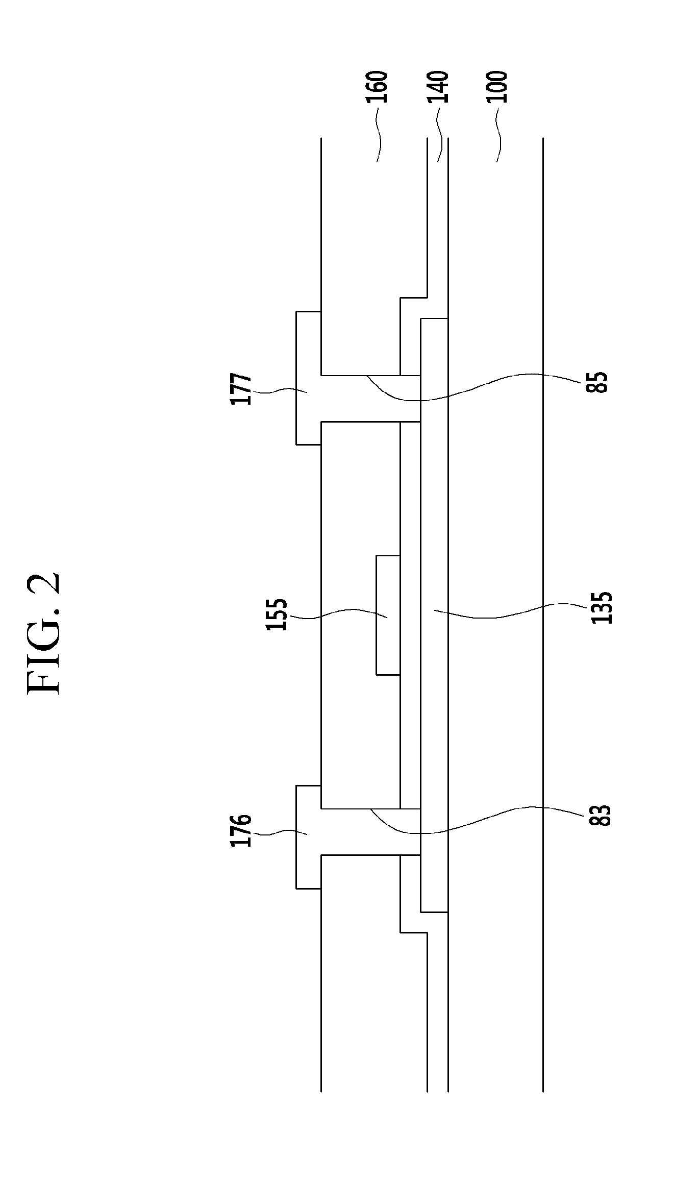
[0048]The exemplary embodiment will be described more fully hereinafter with reference to the accompanying drawings, in which exemplary embodiments are shown. As those skilled in the art would realize, the described exemplary embodiments may be modified in various different ways, all without departing from the spirit or scope of the invention.

[0049]In order to clarify the invention, parts that are not connected with the description will be omitted, and the same elements or equivalents are referred to by the same reference numerals throughout the specification.

[0050]Furthermore, as the size and thickness of the respective structural components shown in the drawings are arbitrarily illustrated for explanatory convenience, the invention is not necessarily limited to as illustrated.

[0051]In the drawings, the thickness of layers, films, panels, regions, etc., are exaggerated for clarity. In the drawings, for better understanding and ease of description, the thicknesses of some layers and...


PUM


Abstract

A thin film transistor includes a semiconductor which is disposed on a substrate and includes a source region, a drain region and a channel region, a gate insulating layer disposed on the semiconductor, a gate electrode disposed on the gate insulating layer, an interlayer insulating layer disposed on the gate electrode, contact holes defined in the interlayer insulating layer, the contact holes respectively exposing the source region and the drain region of the semiconductor, and a source electrode and a drain electrode which are disposed on the interlayer insulating layer and respectively contact the source region and the drain region through the contact holes, where at least one of the contact holes exposing the source region and the drain region obliquely traverses the semiconductor.

Description

[0001]This application claims priority to Korean Patent Application No. 10-2013-0082257 filed on Jul. 12, 2013, and all the benefits accruing therefrom under 35 U.S.C. §119, the entire contents of which are incorporated herein by reference.BACKGROUND[0002]1. Field[0003]The described technology relates generally to a thin film transistor (“TFT”). More particularly, the described technology relates generally to a TFT array panel including a TFT and an organic light emitting diode (“OLED”) display including the same.[0004]2. Description of the Related Art[0005]A thin film transistor (“TFT”) array panel is used as a circuit board to independently drive each pixel in a liquid crystal display or an organic light emitting device (“OLED”).[0006]The TFT array panel includes a gate line transmitting a gate signal, a data line transmitting a data signal, a TFT connected to the gate line and the data line and a pixel electrode connected to the thin film transistor.[0007]The TFT includes a gate ...

Claims


Application Information

Patent Timeline
Patent Type & Authority Applications(United States)
IPC IPC(8): H01L27/32H01L29/786
CPCH01L27/3244H01L29/786H01L27/124H01L27/1248H01L27/1288H01L21/76802H01L29/41733H01L29/78606H01L29/78636H10K59/1213H10K59/131H10K59/123H10K59/35
Inventor LIM, SEA-HEEHONG, SANG-MIN
Owner SAMSUNG DISPLAY CO LTD
Why Eureka
Try Eureka