
A kind of nand string structure and preparation method thereof

A semiconductor and channel layer technology, applied in the direction of semiconductor devices, electrical components, circuits, etc., can solve the problems of large contact resistance, small contact area, difficult alignment, etc., to reduce loss, increase alignment margin, and reduce resistance Effect

Active Publication Date: 2019-02-22
YANGTZE MEMORY TECH CO LTD
View PDF4 Cites 0 Cited by
  • Summary
  • Abstract
  • Description
  • Claims
  • Application Information

AI Technical Summary

Problems solved by technology

[0003] In the current NAND memory manufacturing process, the contact area between the NAND string and other structures is small, resulting in high contact resistance and difficult alignment

Method used


Image

  • A kind of nand string structure and preparation method thereof
  • A kind of nand string structure and preparation method thereof
  • A kind of nand string structure and preparation method thereof

Examples


Embodiment Construction

[0033] Exemplary embodiments of the present disclosure will be described in more detail below with reference to the accompanying drawings. Although exemplary embodiments of the present disclosure are shown in the drawings, it should be understood that the present disclosure may be embodied in various forms and should not be limited by the embodiments set forth herein. Rather, these embodiments are provided for more thorough understanding of the present disclosure and to fully convey the scope of the present disclosure to those skilled in the art.

[0034] It will be understood that, although the terms first, second etc. may be used herein to describe various elements, these elements should not be limited by these terms. These terms are used to distinguish one element from another. For example, a first element could be termed a second element, and, similarly, a second element could be termed a first element, without departing from the scope of the present invention. As used h...


PUM


Abstract

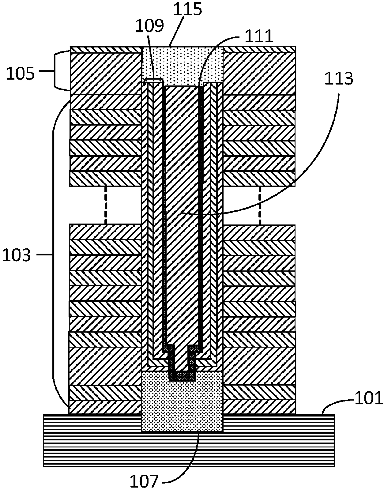
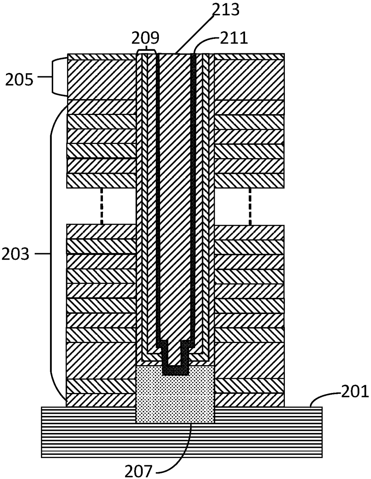
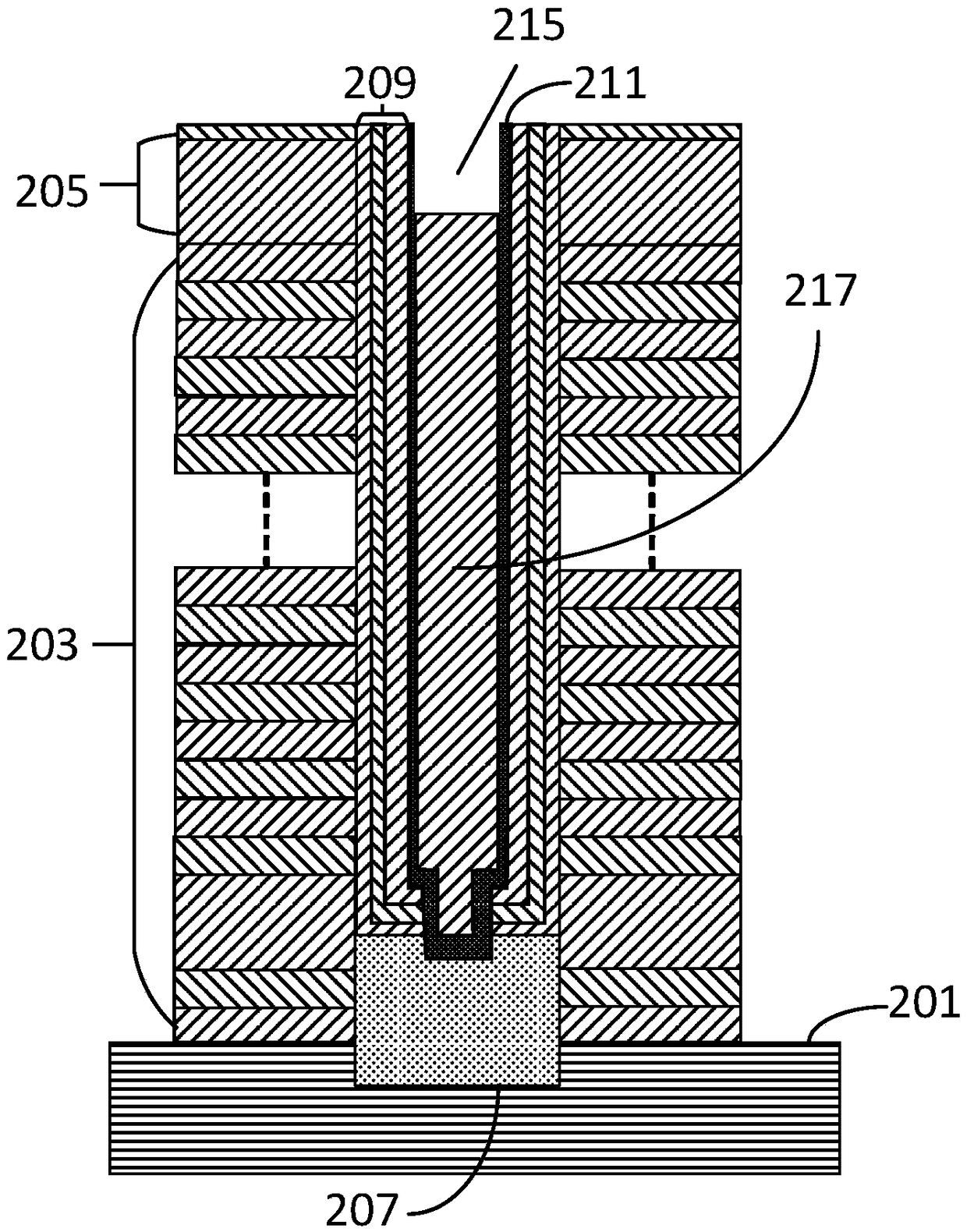
The invention discloses a NAND string structure, comprising a channel hole vertically penetrating through the hierarchical layer stack, a dielectric layer formed in the channel hole, a semiconductor channel layer formed in the dielectric layer, an isolation layer formed in the semiconductor channel layer, and A plugging layer formed at the first end of the channel hole; the plugging layer covers the dielectric layer, the semiconductor channel layer and the isolation layer, and the width or diameter of the plugging layer is larger than the width or diameter of the outer wall of the semiconductor channel layer in contact with it. The present invention reduces the resistance at the top of the NAND string and the contact resistance when the top of the NAND string forms contact with other structures by increasing the critical size of the plug-in layer at the top of the NAND string, and increases the contact resistance at the top of the NAND string when it forms contact with other structures alignment margin.

Description

technical field [0001] The invention relates to a NAND string structure and a preparation method thereof, and belongs to the technical field of 3D NAND memory manufacturing. Background technique [0002] With the continued emphasis on highly integrated electronic devices, there is a continuing need for semiconductor memory devices that operate at higher speeds and lower power and have increased device densities. To this end, devices with smaller dimensions and multilayer devices with transistor cells arranged in horizontal and vertical arrays have been developed. 3D NAND is an emerging type of flash memory developed by the industry. It solves the limitations of 2D or planar NAND flash memory by vertically stacking multi-layer data storage units. It has excellent precision and supports higher capacity in a smaller space. The storage capacity can create a storage device with a storage capacity several times higher than that of similar NAND technologies, thereby effectively re...

Claims


Application Information

Patent Timeline
Patent Type & Authority Patents(China)
IPC IPC(8): H01L27/11524H01L27/11551H01L27/1157H01L27/11578H10B41/35H10B41/20H10B43/20H10B43/35
CPCH10B41/35H10B41/20H10B43/35H10B43/20
Inventor 胡禺石陶谦杨号号董金文陈俊肖莉红吕震宇
Owner YANGTZE MEMORY TECH CO LTD
Learn More