Organic semiconductor compositions

a semiconductor and organic technology, applied in the field of organic copolymer and organic semiconducting compositions, can solve the problems of limited practice, damage to the environment, and the method of preparing the ofets described

Active Publication Date: 2015-01-22
SMARTKEM
View PDF7 Cites 5 Cited by
  • Summary
  • Abstract
  • Description
  • Claims
  • Application Information

AI Technical Summary

Benefits of technology

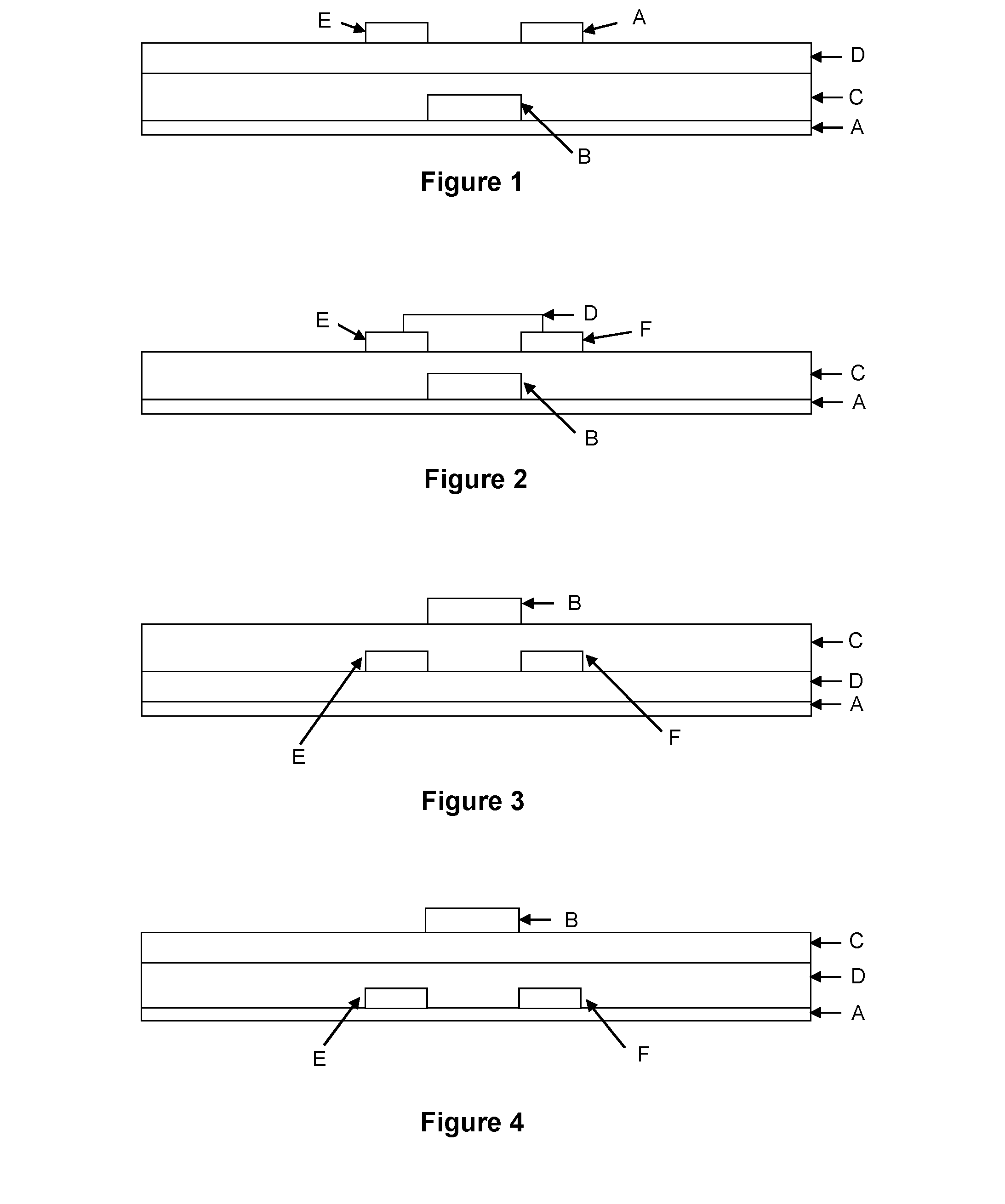
[0146]The rate of removal of the solvent can affect the resulting semiconductor layer. For example, if the removal process is too rapid, poor packing of the semiconductor molecules can occur during crystallisation. Poor packing of the semiconductor molecules can be detrimental to the charge mobility of the semiconductor layer. The solvent can evaporate entirely on its own in an uncontrolled fashion (i.e., no time constraints), or the conditions can be controlled in order to control the rate of evaporation. In order to minimise poor packing, the solvent can be evaporated while slowing the evaporation rate by covering the deposited layer. Such conditions can lead to a semiconductor layer having a relatively high degree of crystallinity.

Problems solved by technology

However the method for preparing the OFETs described in WO 2005 / 055248 in practice is limited and is only useful for producing top gate OFETs having relatively long channel lengths (typically >50 microns).
Moreover these solvents are not ones that would be industrially acceptable in a printing process and these are also damaging to the environment.

Method used


Image

  • Organic semiconductor compositions
  • Organic semiconductor compositions
  • Organic semiconductor compositions

Examples


example 1

PAHC (1): Preparation of TIPS pentacene-9,9-di-n-octylfluorene copolymer

[0223]A mixture of 2,9-dibromo-6,13-bis(triisopropylsilylacetylene)pentacenedione / 2,10-dibromo-6,13-bis(triisopropylsilylacetylene)pentacene(4) (0.15 g, 0.19 mmol, 0.5 eq), 2,7-Dibromo-9.9-di-n-octylfluorene (0.10 g, 0.19 mmol, 0.5 eq), 2,7-bis[(4,4,5,5-tetramethyl-1,3,2-dioxaborolan-2-yl)]-9,9-di-n-octylfuorene(5) (0.24 g, 0.38 mmol, 1 eq) tetrakis(triphenylphosphine)palladium (0) (Acros 12065360, 0.013 g, 0.01 mmol, 0.03 eq), 2M K2CO3 (1.1 mL, 2.23 mmol, 6 eq) and Aliquat® 336 (5 drops) in toluene (20 mL) was degassed by passing a stream of nitrogen through the solution for 30 minutes. The mixture was then heated to reflux. After 3 hours HPLC confirmed the presence of oligomers. The reaction mixture was allowed to cool to 50 deg C. The reaction mixture was poured into MeOH (60 mL) with stirring. After 30 minutes the precipitated solid was collected by filtration under suction using a Buchner funnel to give a d...


PUM

PropertyMeasurementUnit
channel lengthsaaaaaaaaaa
dielectric constantaaaaaaaaaa
channel lengthsaaaaaaaaaa

Abstract

The present invention relates to organic copolymers and organic semiconducting compositions comprising these materials, including layers and devices comprising such organic semiconductor compositions. The invention is also concerned with methods of preparing such organic semiconductor compositions and layers and uses thereof. The invention has application in the field of printed electronics and is particularly useful as the semiconducting material for use in formulations for organic thin film transistor (OTFT backplanes for displays, integrated circuits, organic light emitting diodes (OLEDs), photodetectors, organic photovoltaic (OPV) cells, sensors, memory elements and logic circuits.

Description

FIELD OF THE INVENTION[0001]The present invention relates to organic copolymers and organic semiconducting compositions comprising these materials, including layers and devices comprising such organic semiconductor compositions. The invention is also concerned with methods of preparing such organic semiconductor compositions and layers and uses thereof. The invention has application in the field of printed electronics and is particularly useful as the semiconducting material for use in formulations for organic field effect transistor (OFET) backplanes for displays, integrated circuits, organic light emitting diodes (OLEDs), photodetectors, organic photovoltaic (OPV) cells, sensors, memory elements and logic circuits.BACKGROUND OF THE INVENTION[0002]In recent years, there has been an increasing interest in organic semiconducting materials as an alternative to conventional silicon-based semiconductors. Organic semiconducting materials have several advantages over those based on silico...

Claims


Application Information

Patent Timeline
Patent Type & Authority Applications(United States)
IPC IPC(8): H01L51/00C08G61/02
CPCH01L51/0043C08G61/02C08G2261/95C08G2261/91C08G2261/51H01L51/50C08G2261/12H01L51/42H01L51/0508C08G2261/92C08G2261/3142H01L51/0035C09D165/00H01L51/0541C08G2261/3162C08G2261/314C08K5/01C08G61/126H01L51/0512C08G61/128C08G61/12C08G2261/5222C08G2261/94H01L51/0545H01L2251/30C08G2261/312C08G2261/124H01L51/055C08G2261/3243H01L51/0039Y02E10/549C09D11/52C08G61/10H01L51/0558H10K85/111H10K85/115H10K85/151H10K10/46H10K10/466H10K10/464H10K30/00H10K50/00C08L65/00Y02P70/50H10K85/113H10K10/462H10K10/481H10K10/484H10K2102/00C08G75/06
Inventor GRIFFITHS, RUSSELL, JON
Owner SMARTKEM
Why Eureka
Try Eureka