Power supply device

a power supply and power technology, applied in the direction of power conversion systems, energy saving, climate sustainability, etc., can solve the problems of large circuit size, reduced power supply efficiency, and large switching loss of semiconductor switches, so as to reduce the size and cost of the entire device, and improve the input power factor of the power receiving circuit.

Active Publication Date: 2015-01-22
CENTRAL JAPAN RAILWAY COMPANY +1
View PDF3 Cites 12 Cited by
  • Summary
  • Abstract
  • Description
  • Claims
  • Application Information

AI Technical Summary

Benefits of technology

[0060]In view of the foregoing, the problem to be solved by the present invention is to provide a power supply device that improves an input power factor of a power receiving circuit even during the operation of the power supply device when a resonanc

Problems solved by technology

However, in a power converter which forms a high frequency power source device or a power receiving circuit, the higher the frequency of the current flowing through the circuit, the larger an increase in a switching loss of a semiconductor switch, and a power supply efficiency lowers.
In the non-contact power supply device illustrated in FIG. 8, in particular, a power receiving circuit in a subsequent stage of the resonance capacitor Cr has the following problems.φ Since the power receiving circuit is configured by the full-wave rectifier circuit 10 and the constant voltage control circuit 20, a size of an entire circuit becomes large and it causes an increase in installation space or cost.(2) Since lo

Method used


Image

  • Power supply device
  • Power supply device
  • Power supply device

Examples


first embodiment

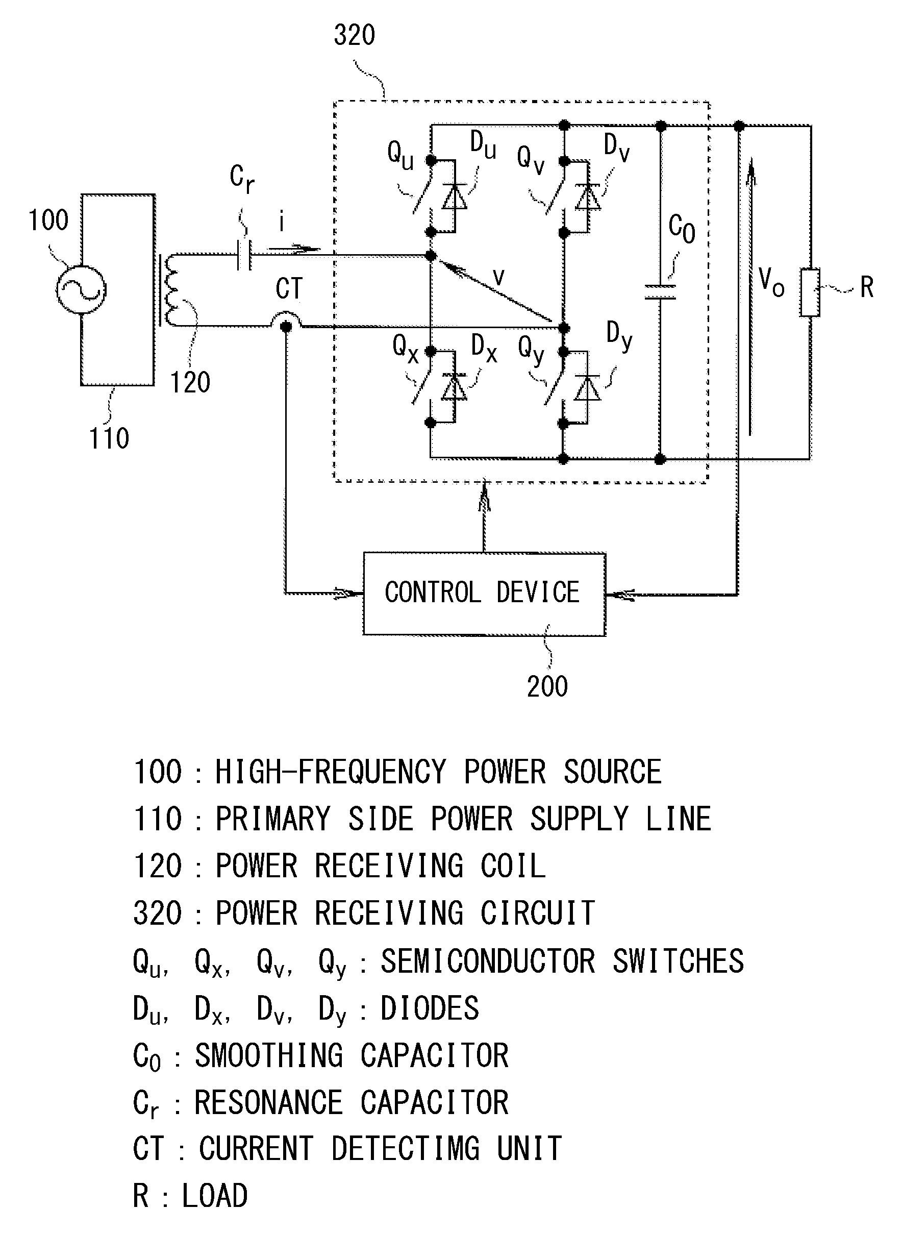
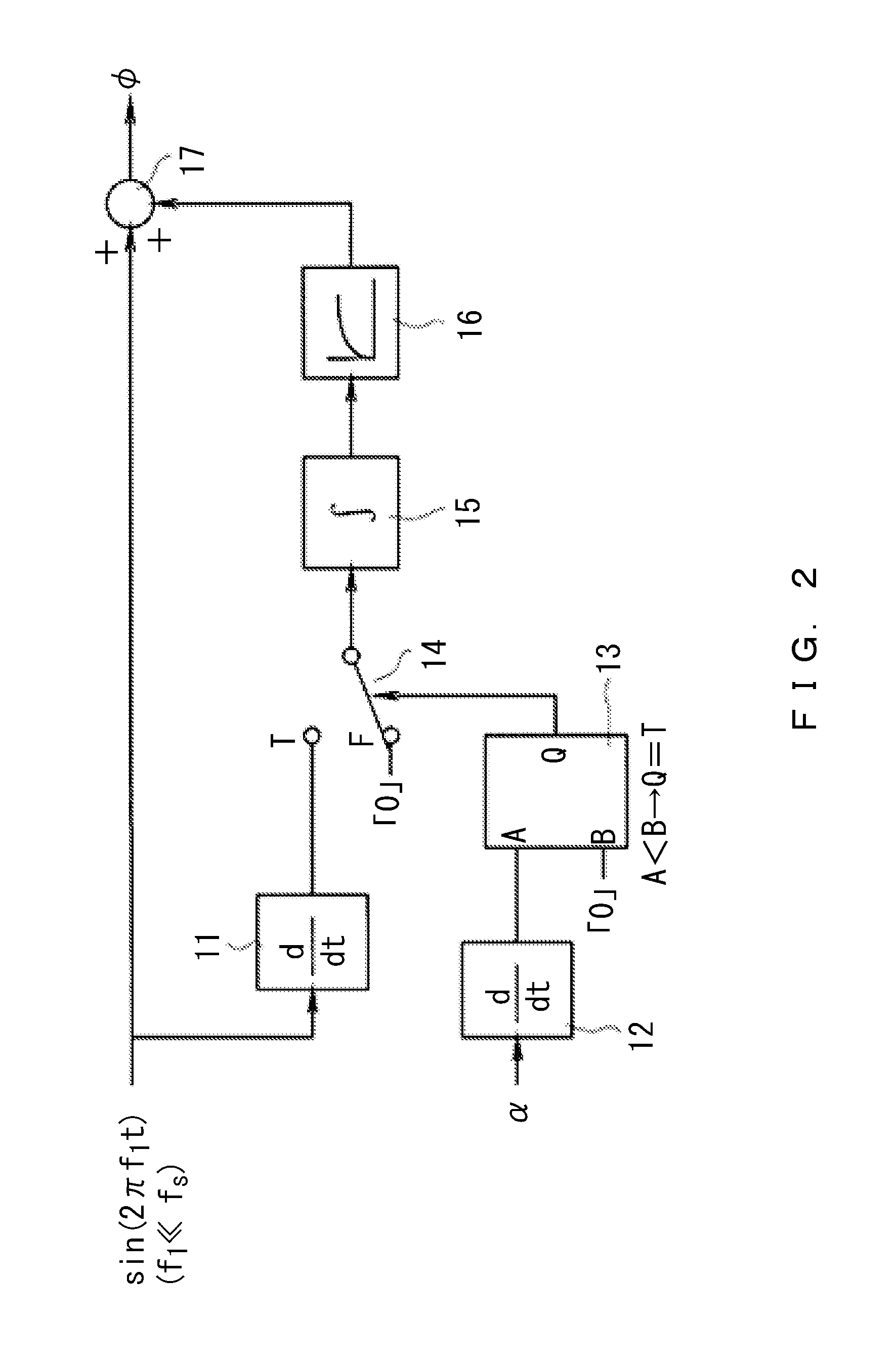
[0093]Described below is a first embodiment on the basis of FIG. 2 and FIG. 3.

[0094]First, in the control block illustrated in FIG. 2, a sine wave input signal sin(2πf1t) for one cycle is provided. A frequency f1 of the sine wave input signal is set to be a sufficiently smaller value than a power source frequency fs, such as about 1 / 10 of fs. When an output of the control block is a compensation period φ from a zero crossing point ZCP of a current i in FIG. 3 (corresponding to a compensation period β in the second prior application invention described above), the period φ is changed with the same frequency f1 as that of the input signal sin(2πf1t). When this happens, as the input signal is changed, a time period α in FIG. 3 is also changed. When the input power factor of the power receiving circuit 320 is low, α becomes long, and when the input power factor is high, α becomes short. A reason for that is described below.

[0095]First, during a time period ii that corresponds to the tim...

second embodiment

[0106]Described next is a second embodiment that corresponds to claim 2.

[0107]FIG. 4 illustrates operating waveforms of a current i that flows through the power receiving coil 120, an induced voltage vin of the power receiving coil 120, a voltage v between AC terminals of a bridge circuit, and a fundamental wave component v′ of the voltage v between the AC terminals of the bridge circuit, and driving signals of switches Qu, Qx, Qv, and Qy, in a case in which the second embodiment is applied to the non-contact power supply circuit illustrated in FIG. 1.

[0108]Details of a route of the current i are omitted, but during time periods forming a time period α (time periods during which the voltage visa zero voltage) I, III, IV, and VI in FIG. 4, the current i flows with a route passing through a power receiving coil 120, a resonance capacitor Cr, and any of the switches Qu, Qx, Qv, and Qy and diodes Du, Dx, Dv, and Dy. During the time periods I, III, IV, and VI, energy is stored in the pow...

third embodiment

[0111]Described next is a third embodiment that corresponds to claim 3.

[0112]FIG. 5 illustrates operating waveforms of a current i that flows through the power receiving coil 120, an induced voltage vin of the power receiving coil 120, a voltage v between AC terminals of a bridge circuit, and a fundamental wave component v′ of the voltage v between the AC terminals of the bridge circuit, and driving signals of switches Qu, Qx, Qv, and Qy, in a case in which the third embodiment is applied to the non-contact power supply circuit illustrated in FIG. 1.

[0113]Details of a route of the current i are omitted, but during time periods forming a time period α (time periods during which the voltage v is a zero voltage) (2) and (3) in FIG. 5, the current i flows with a route passing through a power receiving coil 120, a resonance capacitor Cr, and any of the switches Qu, Qx, Qv, and Qy and diodes Du, Dx, Dv, and Dy. During the time periods (2) and (3), energy is stored in the power receiving c...


PUM


Abstract

In a power supply device, the bridge circuit including a plurality of switching arms which is an inverse-parallel circuit of a semiconductor switch and a diode. The power supply device includes a control unit. The control unit switches the semiconductor switch such that a voltage v between AC terminals becomes a positive-negative voltage whose peak value is the voltage Vo between the DC terminals only during prescribed time periods before and after a point that has deviated from each zero crossing point ZCP of a current i by a prescribed compensation period φ and such that the voltage v between the AC terminals becomes a zero voltage during the other time periods, and sets the compensation period φ such that a time period during which the voltage v between the AC terminals becomes a zero voltage is the shortest.

Description

CROSS REFERENCE TO RELATED APPLICATIONS[0001]This application is based upon and claims the benefit of priority from prior Japanese Patent Application No. 2013-149630, filed Jul. 18, 2013, the entire contents of which are incorporated herein by this reference.BACKGROUND OF THE INVENTION[0002]1. Field of the Invention[0003]The present invention relates to a power supply device that supplies power to a load by utilizing a magnetic coupling between coils.[0004]2. Description of the Related Art[0005]Methods to supply power to a load utilizing a magnetic coupling mutually between coils by electromagnetic induction include, for example, non-contact power supply. The principle thereof is forming a so-called transformer by magnetically coupling a plurality of coils through a space, and utilizing the electromagnetic induction between the coils, thereby exchanging power.[0006]For example, the method includes arranging a primary side coil that corresponds to a power supply source as a power sup...

Claims


Application Information

Patent Timeline
IPC IPC(8): H02M7/219
CPCH02M7/219H02J5/005Y02B70/10H02J50/12H02M1/42H02M1/4258H02M7/5388
Inventor SAWADA, TADASHIMURAI, TOSHIAKIHAGIWARA, YOSHIYASUTOBIKAWA, MASAYUKISAGA, AYAKONISHIJIMA, TOMOTAKAKANEKO, TOSHIYA
Owner CENTRAL JAPAN RAILWAY COMPANY
Why Eureka
Try Eureka