Device with quantum well layer

a quantum well and layer technology, applied in the direction of radiation controlled devices, optical radiation measurement, instruments, etc., can solve the problems of difficult manufacturing of devices with materials of different compositions in the absorbing means and the waveguide, and achieve the effects of reducing losses, reducing absorption in the waveguide, and reducing the band gap of the absorbing layer

Inactive Publication Date: 2015-01-29
ASTRIUM GMBH
View PDF1 Cites 0 Cited by
  • Summary
  • Abstract
  • Description
  • Claims
  • Application Information

AI Technical Summary

Benefits of technology

[0007]The absorbing means may comprise at least one resonator, each or the at least one resonators being resonant at a predetermined wavelength of the electromagnetic radiation. The device may comprise a substrate and the resonators and the waveguide may be provided on the substrate. Ideally, to minimise losses, it is desired to avoid an absorption layer in the waveguide. However, it is difficult to manufacture devices with materials of different compositions in the absorbing means and the waveguide. According to the invention, the quantum-well absorbing layer is provided in both absorbing means and the wavegui

Problems solved by technology

However, it is difficult to manufacture devices with materials of

Method used


Image

  • Device with quantum well layer
  • Device with quantum well layer
  • Device with quantum well layer

Examples


Embodiment Construction

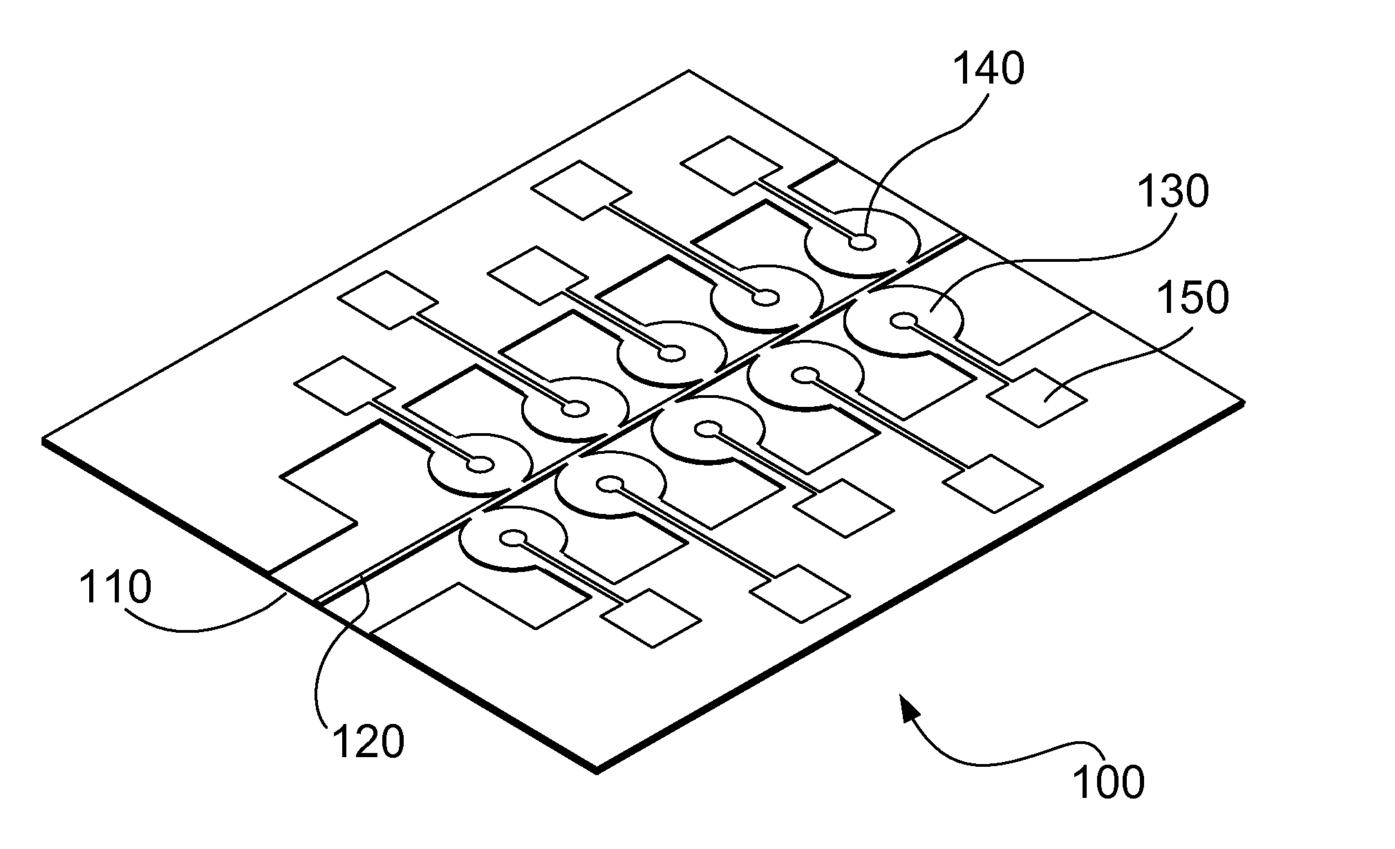
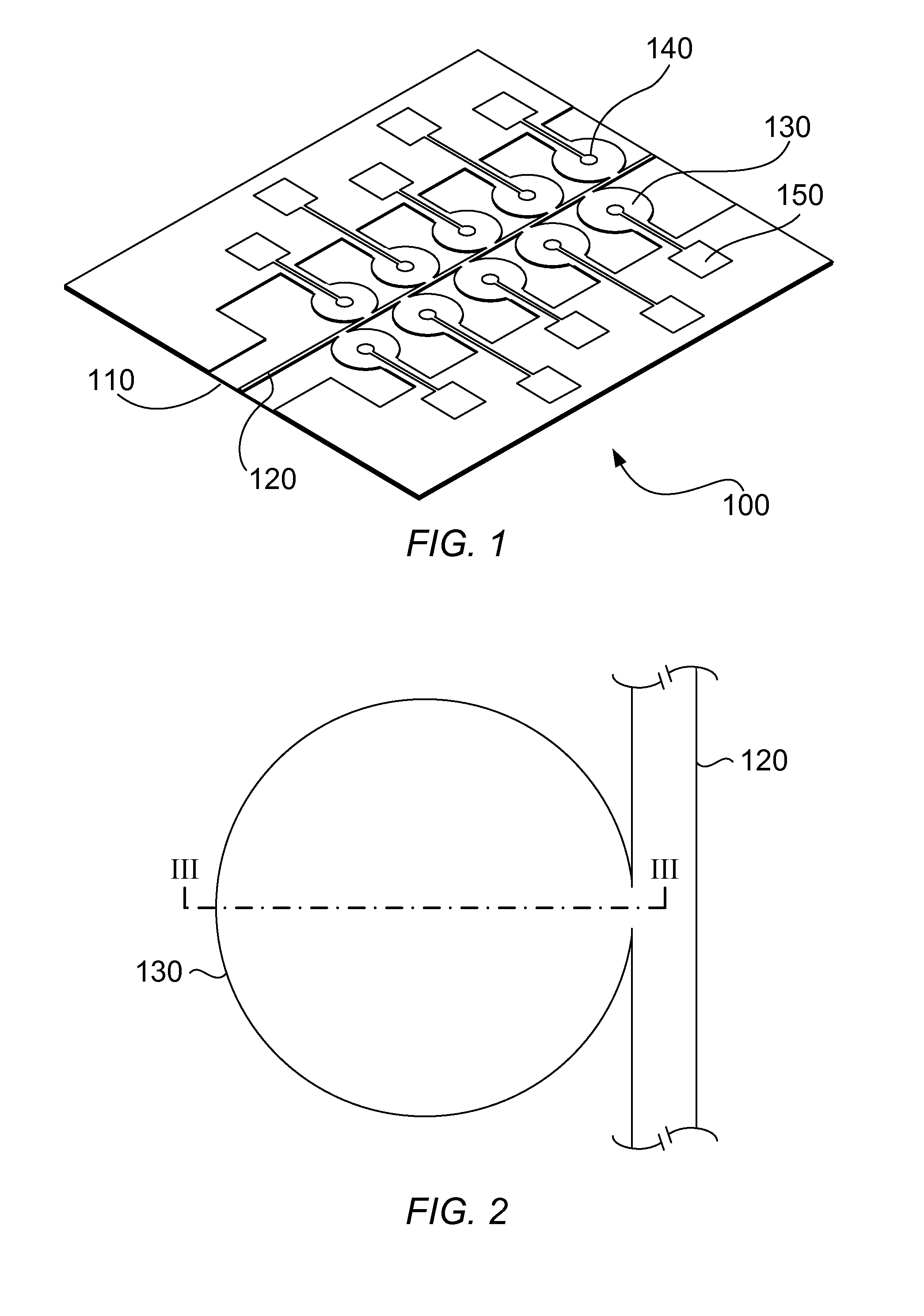
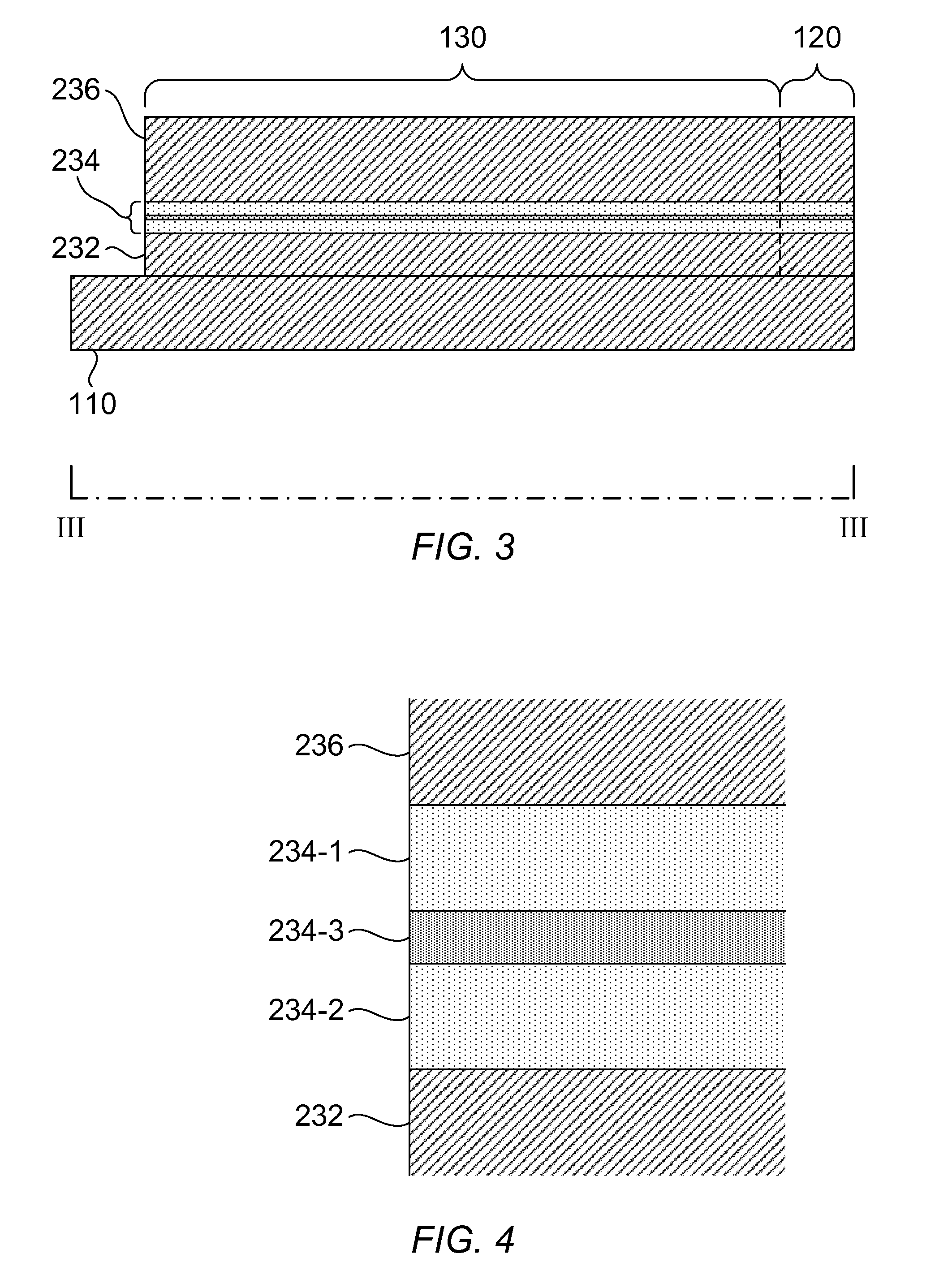
[0025]Referring now to FIG. 1, a spectrometer-on-a-chip is illustrated according to an embodiment of the present invention. The spectrometer 100 comprises a substrate 110, elongate waveguide120, and a plurality of disk resonators 130 coupled to the waveguide 120. The waveguide 120 may be a ridge waveguide. Each disk resonator 130 is provided with an electrode 140 for sensing a current in the disk resonator, the electrode 140 being connected to a bond pad 150 for connecting the spectrometer 100 to other components. One of the disk resonators 130 is shown in plan view in FIG. 2, and FIG. 3 shows a cross-section along the line III-III of FIG. 2. FIG. 4 illustrates in detail the structure of the active layer shown in FIG. 3. The drawings are schematic, and provided for illustrative purposes only. In particular, other layers and components may be present, but have been omitted in the drawings for clarity. For instance, additional layers of metallisation may be deposited above and below t...


PUM


Abstract

A device for guiding and absorbing electromagnetic radiation, the device including: absorbing means for absorbing the electromagnetic radiation; and a coupled to the absorbing means for guiding the electromagnetic radiation to the absorbing means, wherein the waveguide and the absorbing means are formed from a structure including a first cladding layer, a second cladding layer over the first cladding layer, and a quantum-well layer between the first and second cladding layers, the quantum-well layer being formed of a material having a different composition to the first and second cladding layers, wherein the thickness and the composition of the quantum-well layer is optimised to provide an acceptable level of absorption of electromagnetic radiation in the waveguide while providing an appropriate band gap for absorption of the electromagnetic radiation in the absorbing means.

Description

FIELD OF THE INVENTION[0001]The present invention relates to a device for guiding and absorbing electromagnetic radiation. In particular, the invention relates to a structure comprising a quantum-well layer.BACKGROUND OF THE INVENTION[0002]Spectrometers are used in many applications for measuring properties of light across a range of wavelengths. For example, a spectrometer can be used for compositional analysis, by obtaining absorption or emission spectra for an object of interest. The presence and location of peaks within the spectra can indicate the presence of particular elements or compounds. Spectrometers are commonly used for analysis at optical wavelengths, but can also be used at other wavelengths such as microwave and radio wavelengths.[0003]Spectrometers are typically relatively complex and expensive devices that require the alignment of a number of moving parts to be controlled with high precision. For example, a typical spectrometer may focus light onto a diffraction gr...

Claims


Application Information

Patent Timeline
IPC IPC(8): H01L31/0352H01L31/0232H01L27/144G06F17/50
CPCH01L31/035236H01L27/1446H01L31/02325G06F17/5045G02B6/29341G01J3/0205G01J3/42G01J3/0259G02F1/01708B82Y20/00G02F1/0155G06F30/30
Inventor SWEENEY, STEPHENZHANG, YAPING
Owner ASTRIUM GMBH
Why Eureka
Try Eureka