Thin film transistor, organic light-emitting display apparatus including the same, and method of manufacturing the thin film transistor

Inactive Publication Date: 2015-01-29
SAMSUNG DISPLAY CO LTD
View PDF8 Cites 6 Cited by
  • Summary
  • Abstract
  • Description
  • Claims
  • Application Information

AI Technical Summary

Benefits of technology

[0019]According to an exemplary embodiment of the present invention, a thin film transistor including an oxide semiconductor improving both of the mobility and the reliability of materials, an organic li

Problems solved by technology

When the active layer is formed by using the amorphous silicon, carrier mobility may be low, and it may be difficult to obtain a driving circuit having a rapid operation speed.
However a threshold voltage of the thin film transistor may be non-uniform.
In addition, since a common method of forming thin film transistor by using a low temperature polysilic

Method used


Image

  • Thin film transistor, organic light-emitting display apparatus including the same, and method of manufacturing the thin film transistor
  • Thin film transistor, organic light-emitting display apparatus including the same, and method of manufacturing the thin film transistor
  • Thin film transistor, organic light-emitting display apparatus including the same, and method of manufacturing the thin film transistor

Examples


Embodiment Construction

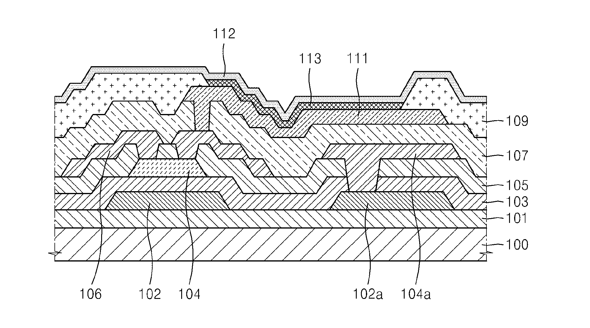
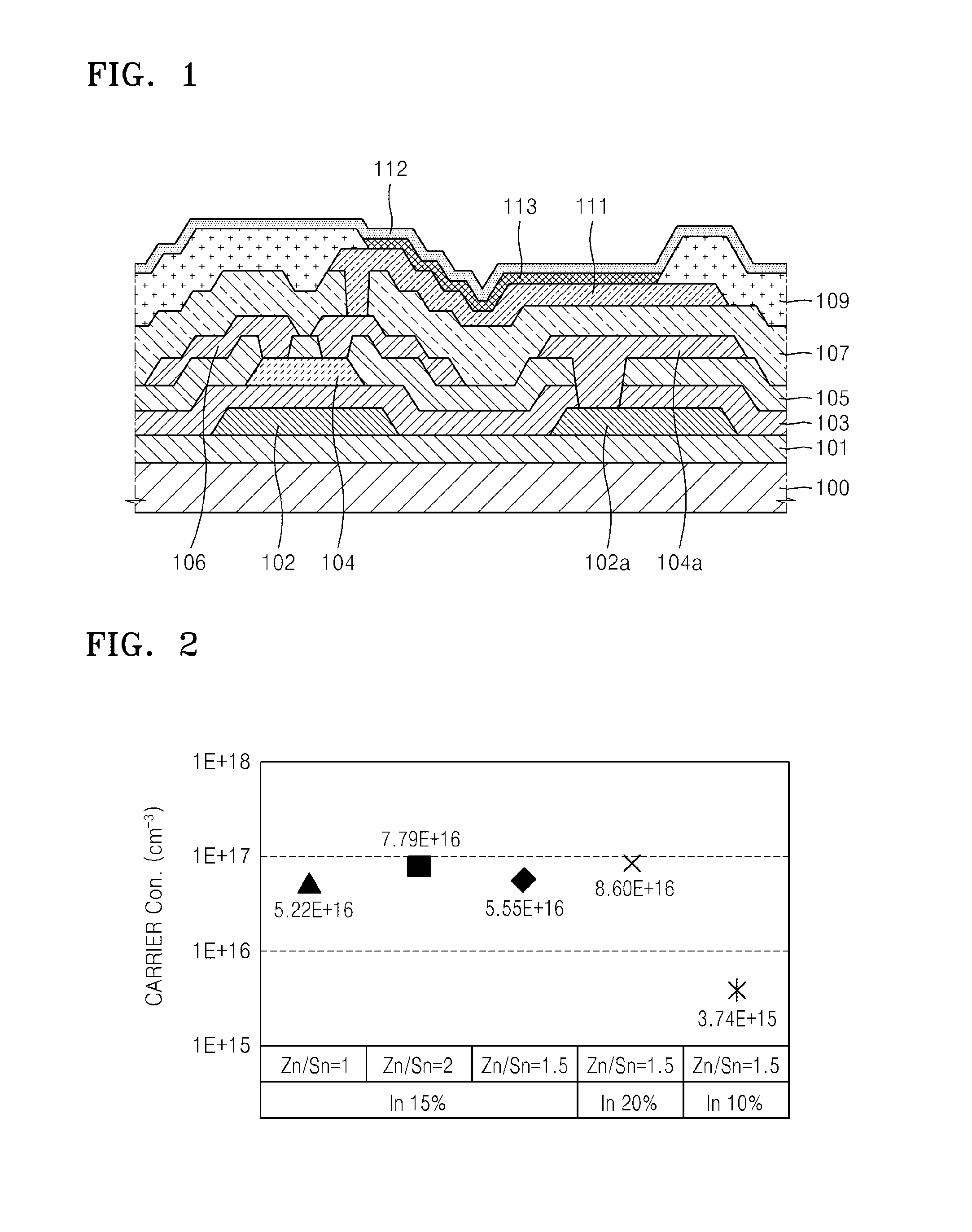
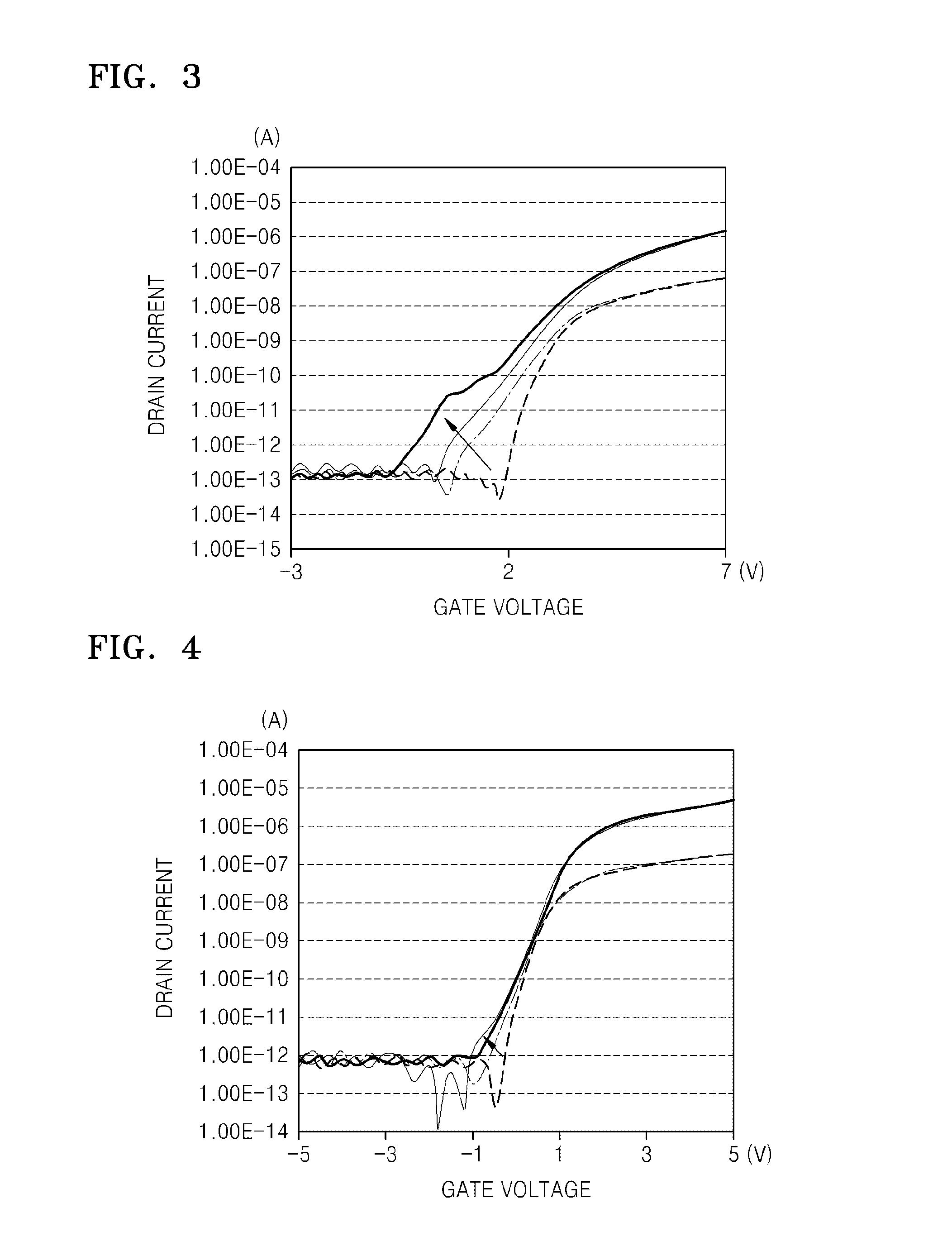
[0025]Hereinafter, embodiments of the inventive concept will be described in detail with reference to the accompanying drawings. Like reference numerals refer to the like elements throughout the specification. The present embodiments may have different forms and should not be construed as being limited to the descriptions set forth herein. Expressions such as “at least one of,” when preceding a list of elements, modify the entire list of elements and do not modify the individual elements of the list.

[0026]Referring to the drawings, the same or corresponding elements will be given the same reference symbols, and duplicated explanation thereon will be omitted.

[0027]As used herein, the singular forms “a,”“an” and “the” are intended to include the plural forms as well, unless the context clearly indicates otherwise. It will be further understood that the terms “comprises” and / or “comprising,” when used in this specification, specify the presence of stated features, elements, and / or comp...


PUM


Abstract

A thin film transistor includes a gate electrode provided on a substrate, a semiconductor layer insulated from the gate electrode and including indium, tin, zinc and gallium oxide, and source/drain electrodes formed on the semiconductor layer.

Description

RELATED APPLICATIONS[0001]This application claims the benefit of Korean Patent Application No. 10-2013-0086975, filed on Jul. 23, 2013, in the Korean Intellectual Property Office, the disclosure of which is incorporated herein in its entirety by reference.BACKGROUND[0002]1. Field[0003]One or more embodiments of the present invention relate to a thin film transistor including an oxide semiconductor, an organic light-emitting display apparatus including the same, and a method of manufacturing the thin film transistor.[0004]2. Description of the Related Art[0005]A flat panel display apparatus such as an organic light-emitting display apparatus, a liquid crystal display apparatus, etc. is manufactured on a substrate including patterns having at least one thin film transistor for driving a pixel, a capacitor, and wirings for connecting the components. The thin film transistor includes an active layer providing a channel region, a source region and a drain region, and a gate electrode for...

Claims


Application Information

Patent Timeline
IPC IPC(8): H01L29/786H01L29/66H01L27/32
CPCH01L29/7869H01L29/66969H01L27/3248H01L27/1225H10K59/1213H01L29/06H01L29/66742
Inventor KIM, KWANG-SUKJEONG, JONG-HANMO, YEON-GON
Owner SAMSUNG DISPLAY CO LTD
Why Eureka
Try Eureka