Manufacture method of AMOLED pixel drive circuit

a manufacturing method and amoled pixel technology, applied in the field of display technology, can solve the problems of poor mobility, high leakage current, poor equality, etc., and achieve the effects of promoting mobility, reducing leakage current, and promoting equality and reliability

Active Publication Date: 2018-08-21
TCL CHINA STAR OPTOELECTRONICS TECH CO LTD
View PDF9 Cites 1 Cited by
  • Summary
  • Abstract
  • Description
  • Claims
  • Application Information

AI Technical Summary

Benefits of technology

[0006]An objective of the present invention is to provide an AMOLED pixel driving circuit, which can reduce the leakage current of the switch thin film transistor and can enhance the mobility and the reliability of the drive thin film transistor to decrease the parasitic capacitance.
[0045]The benefits of the present invention are: in the manufacture method of the AMOLED pixel driving circuit according to the present invention, the oxide semiconductor thin film transistor is utilized to be the switch thin film transistor of the AMOLED pixel driving circuit to reduce the leakage current of the switch thin film transistor, and the P type polysilicon thin film transistor manufactured by utilizing the Solid Phase Crystallization is employed to be the drive thin film transistor of the AMOLED pixel driving circuit to promote the mobility, the equality and the reliability of the drive thin film transistor, and utilizing the P type thin film transistor to be the drive thin film transistor can form the constant current type OLED element, which is more stable than the source follower type OLED formed by the N type thin film transistor, and meanwhile, the parasitic capacitance is decreased with the top gate structure.

Problems solved by technology

Although the mobility of the Low Temperature Poly Silicon (LTPS) thin film transistor based on the Excimer Laser Annealing (ELA) technology is high but the equality is poor, and the leakage current is higher.
On the contrary, the equality of the oxide semiconductor thin film transistor is better, and the leakage current is low but the mobility is lower and the reliability is bad.
Therefore, no matter the oxide semiconductor thin film transistor or the Poly Silicon thin film transistor is utilized, there are defects existing in the present 2T1C AMOLED pixel driving circuit.

Method used


Image

  • Manufacture method of AMOLED pixel drive circuit
  • Manufacture method of AMOLED pixel drive circuit
  • Manufacture method of AMOLED pixel drive circuit

Examples


Embodiment Construction

[0059]For better explaining the technical solution and the effect of the present invention, the present invention will be further described in detail with the accompanying drawings and the specific embodiments.

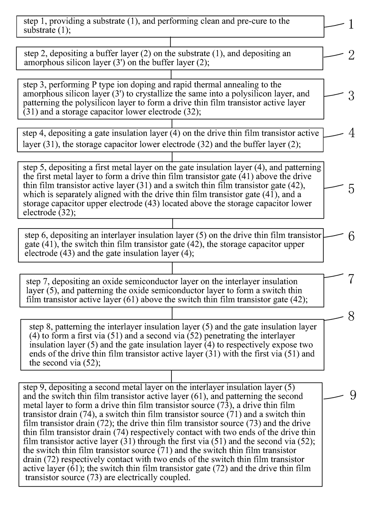
[0060]Please refer to FIG. 11. The present invention provides a manufacture method of an AMOLED pixel driving circuit, comprising steps of:

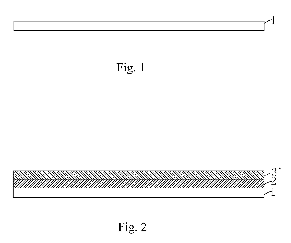
[0061]step 1, referring to FIG. 1, providing a substrate 1, and performing clean and pre-cure to the substrate 1.

[0062]Specifically, the substrate 1 is a transparent substrate and preferably to be a glass substrate.

[0063]step 2, referring to FIG. 2, depositing a buffer layer 2 on the substrate 1, and depositing an amorphous silicon layer 3′ on the buffer layer 2.

[0064]Specifically, material of the buffer layer 2 is one or more combinations of silicon oxide (SiOx) and silicon nitride (SiNx).

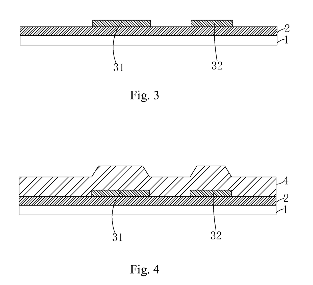
[0065]step 3, referring to FIG. 3, performing P type ion doping and rapid thermal annealing (RTA) to the amorphous silicon layer 3′ to crystallize the sa...


PUM


Abstract

The present invention provides a manufacture method of an AMOLED pixel driving circuit. The method utilizes the oxide semiconductor thin film transistor to be the switch thin film transistor of the AMOLED pixel driving circuit to reduce the leakage current of the switch thin film transistor, and the P type polysilicon thin film transistor manufactured by utilizing the Solid Phase Crystallization is employed to be the drive thin film transistor of the AMOLED pixel driving circuit to promote the mobility, the equality and the reliability of the drive thin film transistor, and utilizing the P type thin film transistor to be the drive thin film transistor can form the constant current type OLED element, which is more stable than the source follower type OLED formed by the N type thin film transistor, and meanwhile, the parasitic capacitance is decreased with the top gate structure.

Description

FIELD OF THE INVENTION[0001]The present invention relates to a display technology field, and more particularly to a manufacture method of an AMOLED pixel drive circuit.BACKGROUND OF THE INVENTION[0002]The Organic Light Emitting Diodes (OLED) display device possesses many outstanding properties of self-illumination, low driving voltage, high luminescence efficiency, short response time, high clarity and contrast, near 180° view angle, wide range of working temperature, applicability of flexible display and large scale full color display. The OLED is considered as the most potential display device.[0003]The OLED can be categorized into two major types according to the driving methods, which are the Passive Matrix OLED (PMOLED) and the Active Matrix OLED (AMOLED), i.e. two types of the direct addressing and the Thin Film Transistor (TFT) matrix addressing. The AMOLED comprises pixels arranged in array and belongs to active display type, which has high lighting efficiency and is general...

Claims


Application Information

Patent Timeline
Patent Type & Authority Patents(United States)
IPC IPC(8): H01L27/12H01L21/02H01L51/00H01L29/167H01L51/52H01L29/66H01L29/24H01L29/49H01L27/32H01L29/786
CPCH01L27/3262H01L21/02043H01L21/02164H01L21/02422H01L21/02532H01L21/02565H01L21/02592H01L21/02667H01L27/1218H01L27/1222H01L27/1225H01L27/1248H01L27/1251H01L27/1255H01L27/1274H01L27/3246H01L27/3248H01L29/167H01L29/24H01L29/66757H01L29/66969H01L29/78675H01L29/78696H01L51/0096H01L51/5206H01L21/0217H01L2251/308H01L27/3258H01L27/3265H01L2227/323H01L27/1259H10K59/12H01L27/124H01L27/127Y02E10/549Y02P70/50H10K59/1213H10K59/1201H10K50/81H10K59/122H10K59/123H10K77/10H10K59/124H10K59/1216H10K2102/103
Inventor ZHOU, XINGYUZHANG, XIAOXINGHSU, YUANJUNZHANG, YADI
Owner TCL CHINA STAR OPTOELECTRONICS TECH CO LTD
Why Eureka
Try Eureka