Crystalline oxide semiconductor thin film, method for producing crystalline oxide semiconductor thin film, and thin film transistor

a technology of crystalline oxide and semiconductor, applied in the direction of crystal growth process, polycrystalline material growth, vacuum evaporation coating, etc., can solve the problems that the variability of tft characteristics cannot be suppressed, and new measures have become necessary, so as to achieve the effect of lowering the mobility

Active Publication Date: 2018-08-02
IDEMITSU KOSAN CO LTD
View PDF3 Cites 1 Cited by
  • Summary
  • Abstract
  • Description
  • Claims
  • Application Information

AI Technical Summary

Benefits of technology

[0101]In the same manner as in the TFT production process, a 50 nm-oxide semiconductor film was formed on a glass substrate, followed by a heat treatment. Then, the film was cut into a 1 cm×1 cm square. At the four corners, gold (Au) was deposited by means of an ion coater by using a metal mask in a size of 2 mm×2 mm or less.
[0102]As the glass substrate, ABC-G manufactured by Nippon Electric Glass Co., Ltd. was used.
[0103]The sample for measuring hall effect was set in a hall effect specific resistance measurement apparatus (ResiTest 8300, manufactured by Toyo Corporation), the hall effect was evaluated at room temperature, whereby the carrier density and the mobility were obtained. The results are shown in Table 1-1.
[0104]On the semiconductor film for measuring the hall effect, a SiO2 film was formed by a CVD apparatus, hall measurement was conducted. After the heat treatment, hall measurement was conducted. The results are shown in Table 1-1.
[0105]The crystalline property of the unheated film and the heated film after the sputtering (after film deposition) was evaluated by an X-ray diffraction (XRD) measurement, it was revealed that the film was amorphous before the heating and the film was crystalline (bixbyite structure) after the heating. The lattice c

Problems solved by technology

For example, when an oxide thin film is crystallized by heating at a rapid temperature-elevation speed, crystal growth occurs radially, whereby the crystal orientation becomes radial, and a large number of lattice defects causing the carrier density variation are formed in the inside of a crystal grai

Method used


Image

  • Crystalline oxide semiconductor thin film, method for producing crystalline oxide semiconductor thin film, and thin film transistor
  • Crystalline oxide semiconductor thin film, method for producing crystalline oxide semiconductor thin film, and thin film transistor
  • Crystalline oxide semiconductor thin film, method for producing crystalline oxide semiconductor thin film, and thin film transistor

Examples


example 1

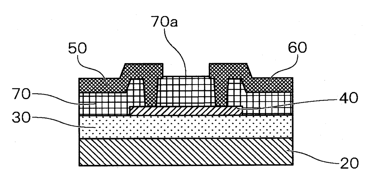
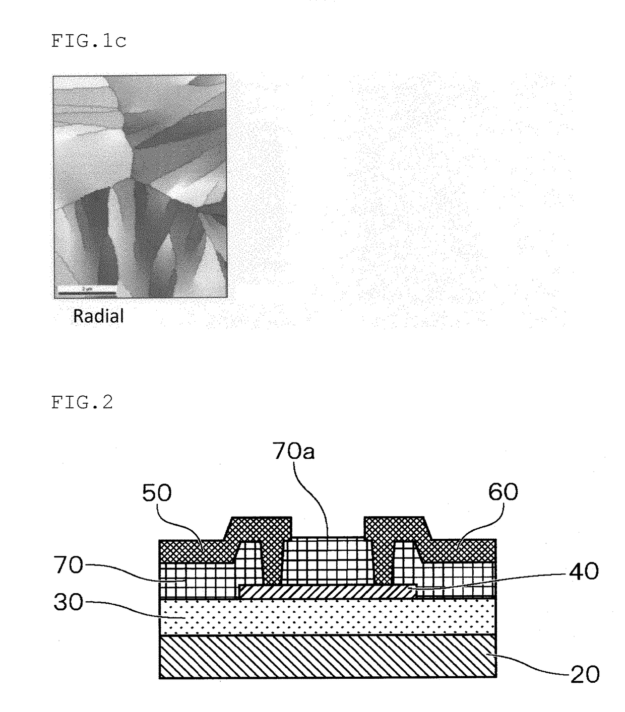
[0095]The thin film transistor having a structure shown in FIG. 2 was produced by the following steps:

(1) Film-Forming Step

[0096]By sputtering using a sputtering target obtained by mixing 96 wt % (89.8 at %) of indium oxide and 4 wt % (10.2 at %) of aluminum oxide, on a silicon wafer (gate electrode 20) with a thermally oxidized film (gate insulating film 30), a 50 nm-thick thin film (oxide semiconductor layer 40) was formed through a metal mask. As the sputtering gas, a mixed gas of high-purity argon and high-purity oxygen (concentration of impurities: 0.01 vol %) was used, and sputtering was conducted under the film-forming conditions shown in Table 1-1.

(2) Heating Step

[0097]The obtained stacked body was subjected to a heat treatment in the air at the temperature, the time and the conditions shown in Table 1-1. The “heat treatment after film formation: time (min)” in the “heat treatment conditions after the formation of the semiconductor film” in Table 1-1 means the time taken fro...

examples 10 and 11

[0123]Thin film transistors were produced in the same manner as in Example 1, except that semiconductor thin films were formed by using the sputtering targets having compositions shown in Table 2 and a heat treatment or the like were conducted, and properties of a TFT were evaluated.

[0124]Further, in the same manner as in Example 1, for a sample on which only an oxide thin film was mounted on a glass substrate, hall measurements were conducted at each stage in Table 2. An increase or decrease in carrier density and band gap were measured, and the results are shown in Table 2.

[0125]In the atomic ratio of the sputtering targets shown in the table, the numerical value shown by the “wt %” indicates the weight ratio (charged amount) of indium oxide, gallium oxide, yttrium oxide and tin oxide, the numerical value indicated by the “at %” indicates an indium element, a gallium element, an yttrium element and a tin element.

[0126]The “E+XX” in the table means “1×10+XX”.

[0127]The “ratio of the...

examples 12 and 13

[0128]Thin film transistors were produced in the same manner as in Example 1, except that semiconductor thin films were formed by using sputtering targets having the compositions shown in Table 3 and a heat treatment or the like were conducted, and properties of a TFT were evaluated.

[0129]In the same manner as in Example 1, for a sample on which only an oxide thin film was mounted on a glass substrate, hall measurement was conducted at each stage shown in Table 3, and an increase or decrease of carrier density and band gap were measured. The results are shown in Table 3.

[0130]In the atomic ratio of the sputtering target in the table, the numerical value indicated by “wt %” shows the weight ratio (charged amount) of indium oxide, gallium oxide, samarium oxide and tin oxide, and the numerical value indicated by “at %” shows the atomic value of an indium element, a gallium element, a samarium element and a tin element.

[0131]The “E+XX” in the table means “1×10+XX”.

[0132]The “ratio of th...


PUM

PropertyMeasurementUnit
Temperatureaaaaaaaaaa

Abstract

A crystalline oxide semiconductor thin film that is composed mainly of indium oxide and comprises surface crystal grains having a single crystal orientation.

Description

TECHNICAL FIELD[0001]The invention relates to a crystalline oxide semiconductor thin film. In particular, the invention relates to a crystalline oxide semiconductor thin film of a thin film transistor (TFT) used in a display such as a liquid crystal display or an organic EL display. The crystalline oxide semiconductor thin film of the invention can be preferably used in a solar cell, a display such as a liquid crystal element, an organic electroluminescence element and an inorganic electroluminescence element, and an electronic device such as a power semiconductor device and a touch panel. These can be preferably used in an electric device or a vehicle.BACKGROUND ART[0002]An amorphous oxide semiconductor used in a TFT has a higher carrier mobility as compared with a general-purpose amorphous silicon (a-Si), has a large optical band gap and can be formed into a film at lower temperatures, and hence, is expected to be applied to a next-generation display that requires an increase in s...

Claims


Application Information

Patent Timeline
IPC IPC(8): H01L29/786C01G15/00C23C14/08C23C14/34C23C14/58C30B1/02C30B29/16H01L29/24H01L29/04H01L21/02H01L29/66
CPCH01L29/7869C01G15/00C23C14/086C23C14/34C23C14/5806C30B1/023C30B29/16H01L29/24H01L29/04H01L21/02565H01L21/02631H01L29/66969H01L21/02592H01L21/02667C01P2006/40C01P2002/54C01P2002/70H01L21/02595C23C14/08C01P2004/61H01L29/78618H01L29/78603H01L21/324
Inventor INOUE, KAZUYOSHIUTSUNO, FUTOSHITSURUMA, YUKITOMAI, SHIGEKAZUEBATA, KAZUAKI
Owner IDEMITSU KOSAN CO LTD
Why Eureka
Try Eureka