Check patentability & draft patents in minutes with Patsnap Eureka AI!

High voltage input circuit for a differential amplifier

Active Publication Date: 2015-01-29
TEXAS INSTR INC
View PDF2 Cites 3 Cited by
  • Summary
  • Abstract
  • Description
  • Claims
  • Application Information

AI Technical Summary

Benefits of technology

The patent describes a circuit that allows for differential input. It includes four transistors that have different control terminals and current paths. The circuit allows for the simultaneous input of two signals through the same circuit, which can be useful for certain applications. The technical effect of this invention is to provide a more complex and versatile circuit for handling input signals in a differential way.

Problems solved by technology

These diode clamps, however, conduct high currents under forward bias.
Moreover, they increase input capacitance, may slow operation due to forward bias recovery time, and increase noise.
However, there are several disadvantages to this circuit.
This increases noise and offset voltage and decreases bandwidth of the differential amplifier.

Method used


Image

  • High voltage input circuit for a differential amplifier
  • High voltage input circuit for a differential amplifier
  • High voltage input circuit for a differential amplifier

Examples


first embodiment

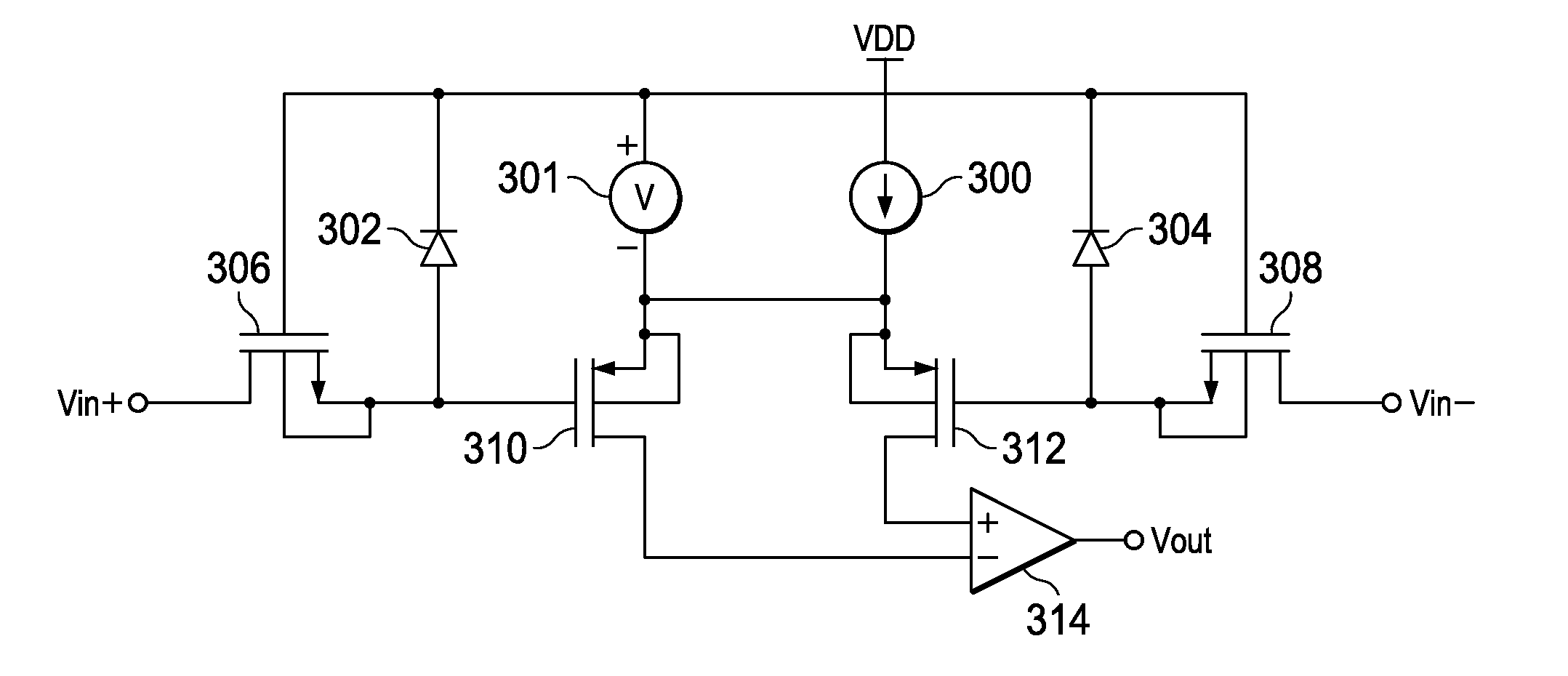
[0020]Referring to FIG. 3A, there is a circuit diagram of a high voltage differential amplifier circuit of the present invention. Here and in the following discussion, the same reference numerals are used in the drawing figures to indicate substantially the same circuit elements. The circuit includes differential amplifier 314 having output terminal Vout. The differential amplifier may be an operational amplifier configured as a linear amplifier, integrator, or other special purpose amplifier as is known in the art. The differential amplifier 314 has first (−) and second (+) input terminals. A first p-channel input transistor 310 has a current path coupled to the first (−) input terminal. A second p-channel input transistor 312 has a current path coupled to the second (+) input terminal. The first and second input transistors are preferably balanced and have substantially the same threshold voltage and are oriented to compensate for any slight misalignment during fabrication. N-chan...

second embodiment

[0023]Turning now to FIG. 4A, there is a circuit diagram of a high voltage differential amplifier circuit of the present invention. The circuit includes differential amplifier 314 having output terminal Vout. The differential amplifier 314 has first (−) and second (+) input terminals. A first p-channel input transistor 316 has a current path coupled to the first (−) input terminal. A second p-channel input transistor 318 has a current path coupled to the second (+) input terminal. The first and second input transistors are preferably balanced and have substantially the same threshold voltage and are oriented to compensate for any slight misalignment during fabrication. N-channel transistor 306 has a current path coupled between a first differential input terminal (Vin+) and a control terminal of the first input transistor 316. N-channel transistor 308 has a current path coupled between a second differential input terminal (Vin−) and a control terminal of the second input transistor ...

third embodiment

[0025]Turning now to FIG. 5A, there is a circuit diagram of a high voltage differential amplifier circuit of the present invention. The circuit includes differential amplifier 314 having output terminal Vout. The differential amplifier 314 has first (−) and second (+) input terminals. A first p-channel input transistor 310 has a current path coupled to the first (−) input terminal. A second p-channel input transistor 312 has a current path coupled to the second (+) input terminal. The first and second input transistors are preferably balanced and have substantially the same threshold voltage and are oriented to compensate for any slight misalignment during fabrication. N-channel transistor 306 has a current path coupled between a first differential input terminal (Vin+) and a control terminal of the first input transistor 310. N-channel transistor 308 has a current path coupled between a second differential input terminal (Vin−) and a control terminal of the second input transistor ...


PUM


Abstract

A differential input circuit (FIG. 3A) is disclosed. The circuit includes a first input terminal (drain of 310) and a second input terminal (drain of 312). A first input transistor (310) has a first control terminal and has a current path coupled to the first input terminal. A second input transistor (312) has a second control terminal and has a current path coupled to the second input terminal. A third transistor (306) has a third control terminal and has a current path between a first differential input terminal (Vin+) and the first control terminal. A fourth transistor (308) has a fourth control terminal and has a current path between a second differential input terminal (Vin−) and the second control terminal.

Description

BACKGROUND OF THE INVENTION[0001]Embodiments of the present invention relate to a high voltage input stage for a complementary metal oxide semiconductor (CMOS) differential amplifier.[0002]High voltage differential amplifiers using relatively low voltage transistors require protection for differential input terminals to avoid gate oxide stress. Circuits of the prior art have typically used diode clamps to limit peak-to-peak voltage across differential input terminals. These diode clamps, however, conduct high currents under forward bias. Moreover, they increase input capacitance, may slow operation due to forward bias recovery time, and increase noise.[0003]Referring to FIG. 1, there is a high voltage differential amplifier circuit of the prior art. Here, and in the following discussion the differential amplifier may be an operational amplifier or other balanced amplifier for amplifying difference signals. The circuit includes back-to-back diodes 102 and 104 connected between differ...

Claims


Application Information

Patent Timeline
IPC IPC(8): H03F3/45H03F1/02
CPCH03F1/0211H03F3/45179H03F3/45376H03F2203/45568H03F2203/45571
Inventor BRANTLEY, STEVEN GRAHAMIVANOV, VADIM VALERIEVICH
Owner TEXAS INSTR INC
Features
  • R&D
  • Intellectual Property
  • Life Sciences
  • Materials
  • Tech Scout
  • Unparalleled Data Quality
  • Higher Quality Content
  • 60% Fewer Hallucinations
Learn More