Monolithic IGBT and diode structure for quasi-resonant converters

a quasi-resonant converter and monolithic igbt technology, applied in the direction of diodes, semiconductor devices, semiconductor/solid-state device details, etc., can solve the problems of increasing manufacturing costs, increasing resistance, and difficulty in conventional technologies for configuring and manufacturing quasi-resonant converters as power devices. achieve the effect of improving the production cost and the form factor of the quasi-resonant converter

Active Publication Date: 2015-02-05
ALPHA & OMEGA SEMICON INC
View PDF4 Cites 9 Cited by
  • Summary
  • Abstract
  • Description
  • Claims
  • Application Information

AI Technical Summary

Benefits of technology

[0009]It is therefore an aspect of the present invention to provide a new and improved device configuration and manufacturing method for providing a monolithic IGBT combined with a lateral diode structure without requiring a co-packaging of an IGBT die with a separate diode die and without requiring backside processing steps on a wafer to form the anti-parallel diode. The production cost and form factor of the quasi-resonant converter are therefore improved.

Problems solved by technology

Conventional technologies to configure and manufacture quasi-resonant converters as power devices still have difficulties and limitations.
The manufacturing costs are increased due to this requirement to assemble and connect two separate dies (IGBT and diode) as a co-packaged assembly.
This increases the resistance and reduces the current handling capability of the device.
These additional backside processing steps cause the production cost to increase, and are more difficult to carry out.
In cases with thin wafer processing, additional backside processing steps with the thinned wafer also increase the risk of wafer damage.
Also, with the reverse conducting vertical diode configuration, as shown in FIG. 1C, the device may suffer from snapback during device turn-on.

Method used


Image

  • Monolithic IGBT and diode structure for quasi-resonant converters
  • Monolithic IGBT and diode structure for quasi-resonant converters
  • Monolithic IGBT and diode structure for quasi-resonant converters

Examples


Embodiment Construction

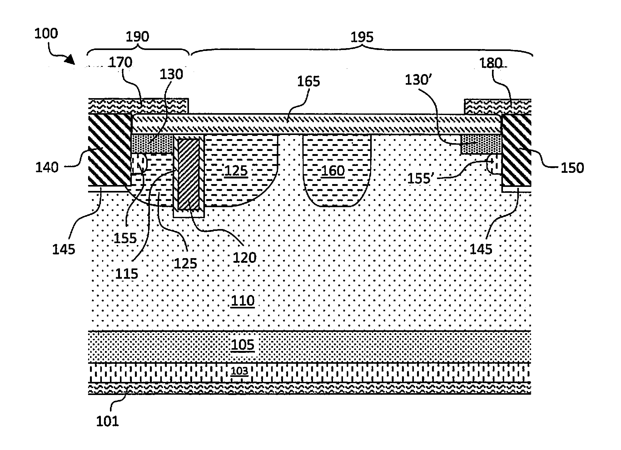
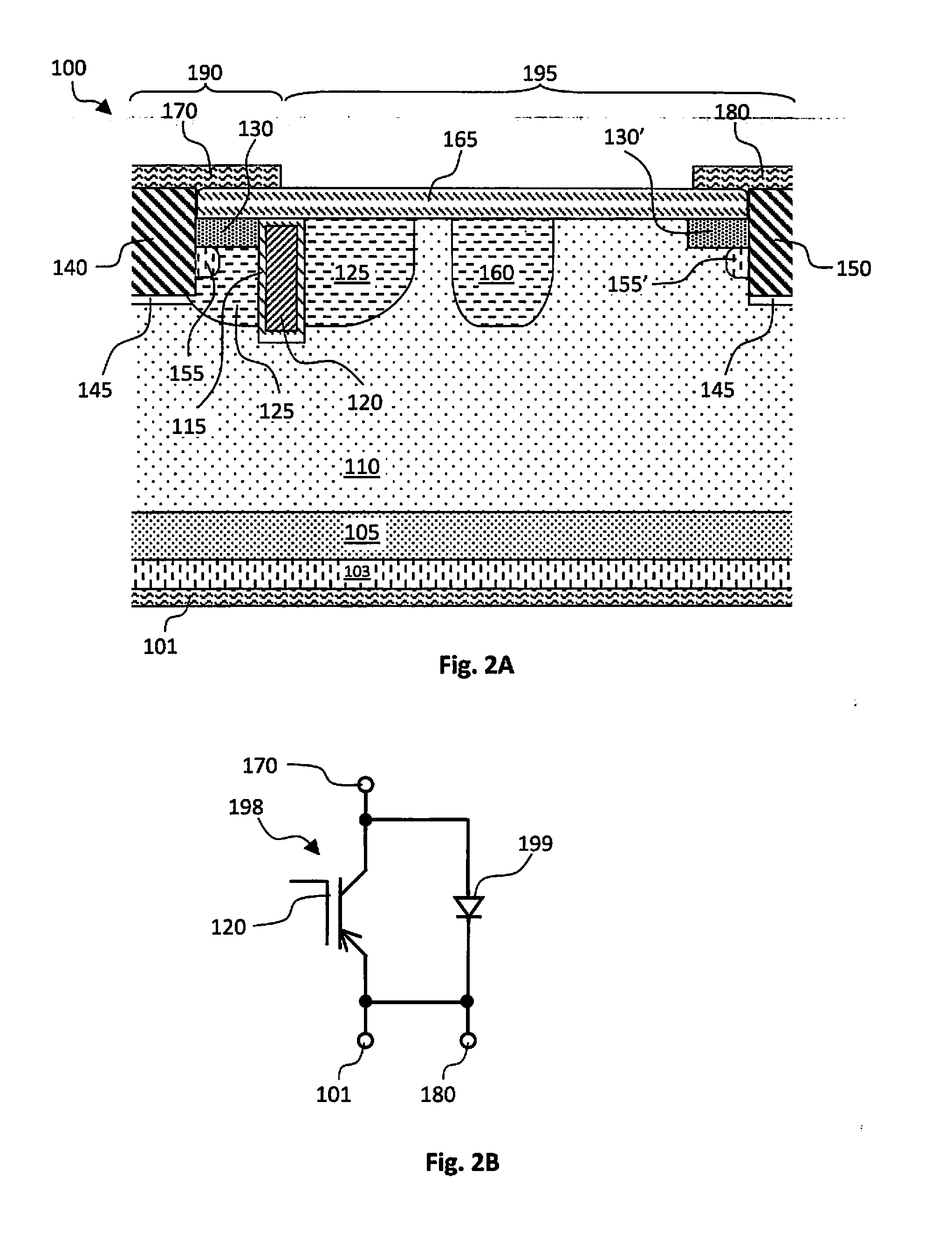
[0026]FIG. 2A is a cross-sectional view that shows a vertical insulated gate bipolar transistor (IGBT) integrated with a lateral diode structure of this invention as IGBT die 100. By way of example, the IGBT may include a trench metal oxide semiconductor (MOS) gate structure with a lateral diode. The combined trench MOS structure with the lateral diode is formed in a semiconductor substrate with a collector terminal 101 attached to a backside surface underneath a P-type collector layer 103 disposed at the bottom of the substrate. The substrate includes an N-type layer located over the P-type collector 103; by way of example, and as shown in FIG. 2A, this N-type layer may comprise an N-type field stop layer 105 located over the P-type collector 103, and a lightly doped N-type layer 110 (e.g. an N-type epitaxial layer) located over the N-type field stop layer 105. The N-type buffer layer 105 is more heavily doped than the N-type layer 110. The combined IGBT with a lateral diode may fu...


PUM


Abstract

This invention discloses a semiconductor power device formed in a semiconductor substrate. The semiconductor power device further includes a channel stop region near a peripheral of the semiconductor substrate wherein the channel stop region further includes a peripheral terminal of a diode corresponding with another terminal of the diode laterally opposite from the peripheral terminal disposed on an active area of the semiconductor power device. In an embodiment of this invention, the semiconductor power device is an insulated gate bipolar transistor (IGBT).

Description

[0001]This is a Divisional application of a previously filed co-pending application with Ser. No. 12 / 928,988 filed on Aug. 6, 2013 by identical common inventors of this Application. The disclosures made in application Ser. No. 12 / 928,988 are hereby incorporated by reference in this patent application.BACKGROUND OF THE INVENTION[0002]1. Field of the Invention[0003]The invention relates generally to semiconductor power devices. More particularly, this invention relates to new configurations and methods for manufacturing improved quasi-resonant converters by combining an insulated gate bipolar transistor (IGBT) with a lateral diode as a monolithic structure and a packaging configuration without a requirement of co-packaging a separate diode die and without a requirement of specialized wafer backside process.[0004]2. Description of the Prior Art[0005]Conventional technologies to configure and manufacture quasi-resonant converters as power devices still have difficulties and limitations....

Claims


Application Information

Patent Timeline
Patent Type & Authority Applications(United States)
IPC IPC(8): H01L27/06H01L21/8248
CPCH01L21/8248H01L27/0629H01L2224/0603H01L2224/48137H01L2224/48247H01L29/7395H01L2924/13055H01L29/7397H01L29/0619H01L29/1095H01L29/423H01L29/6634H01L29/66348H01L29/0638H01L23/4952H01L23/49562H01L2924/181H01L2924/00H01L2924/00012
Inventor BHALLA, ANUP
Owner ALPHA & OMEGA SEMICON INC
Why Eureka
Try Eureka