

Switching power supply control circuit
a control circuit and power supply technology, applied in the direction of power conversion systems, dc-dc conversion, instruments, etc., can solve problems such as complicated phase compensation circuits, achieve the effects of reducing output voltage oscillation, improving response, and facilitating comparing detection values
- Summary
- Abstract
- Description
- Claims
- Application Information
AI Technical Summary
Benefits of technology
Problems solved by technology
Method used
Image

Examples
first embodiment
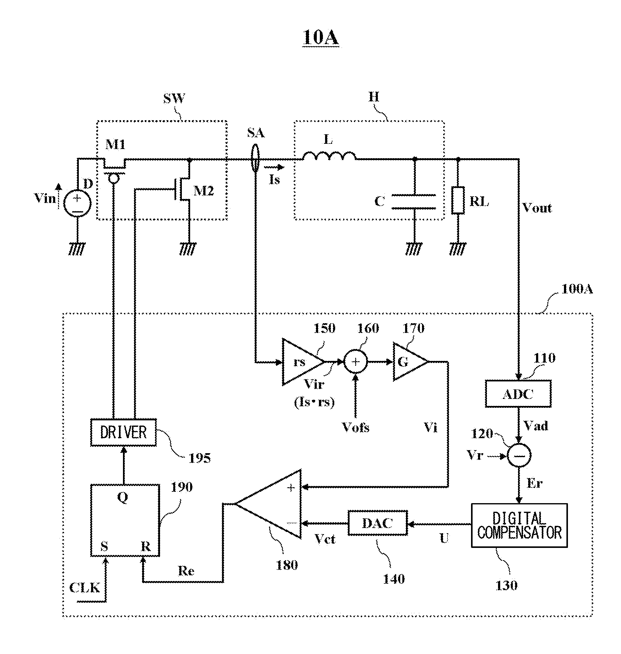
[0025]FIG. 1 shows a switching power supply control circuit according to the first embodiment of the present invention, and in particular, shows a pulse width modulation (PWM) current mode step-down switching regulator.
[0026]The switching power supply control circuit 10A in FIG. 1 has a switching element SW, a smoothing circuit H, and a switching controller 100A. A current sensor SA, configured to detect an output current Is, is disposed between the switching element SW and the smoothing circuit H.
[0027]The switching element SW can divide a direct current generated by a DC power source D, and is provided with a p-channel field effect transistor M1 and a n-channel field effect transistor M2.
[0028]The smoothing circuit H can smooth the direct current divided by the switching element SW, and is provided with an inductor L and a capacitor C.
[0029]The source of the p-channel field effect transistor M1 is connected to the DC power source D, to which an input voltage Vin is applied, the dr...
second embodiment
[0068]FIG. 7 shows a switching power supply control circuit 10B according to a second embodiment of the present invention. The difference from the first embodiment (FIG. 1) is that a switching controller 100B has an operational amplifier 170A comprising an amplifier between the I-V converter 150 and the analog comparator 180. Specifically, the operational amplifier 170A shown in FIG. 7 has the functions of both the adder 160 and the amplifier 170 shown in FIG. 1. The circuit structure can be simplified by inputting the I-V conversion voltage Vir to a non-inverting input terminal of the operational amplifier 170A, and applying the offset voltage Vofs to this inverting input terminal.
third embodiment
[0069]FIG. 8 shows a switching power supply control circuit 10C according to a third embodiment of the present invention. The difference from the first embodiment (FIG. 1) is that a switching controller 100C is designed such that a DAC 610 generates the offset voltage Vofs, and therefore, a high-order bit U_msb of the digital compensation value U outputted by the digital compensator 130 is inputted to the DAC 610. The switching controller is also designed such that the DAC 140 converts a low-order bit U_lsb of the digital compensation value U from digital to analog, and the converted output signal Vct 1 is inputted to an inverting input terminal of the analog comparator 180. With the third embodiment, the offset voltage Vofs was generated on the basis of the high-order bit U_msb of the digital compensation value U, the low-order bit U_lsb of the digital compensation value U was converted from digital to analog by the DAC 140, and the converted valued was inputted to the analog compa...
PUM
 Abstract
Description
Claims
Application Information