Light source circuit and light source device equipped with same

Active Publication Date: 2015-02-05
NEC CORP +1
View PDF1 Cites 9 Cited by
  • Summary
  • Abstract
  • Description
  • Claims
  • Application Information

AI Technical Summary

Benefits of technology

The present invention relates to a new way of reducing unwanted light in a light source circuit, which can affect the operation of a laser diode. By combining the reflection light from previous optical branches in an anti-phased state, the invention effectively inhibits the returning light and stabilizes the operation of the laser diode.

Problems solved by technology

It is known that silicon is an indirect transition type material, and thus a light source with high energy efficiency is difficult to be realized using the silicon.
When the returning light is incident on the laser diode, a variation in output intensity of the laser diode (that is, generation of an intensity noise) or a variation in emission wavelength (generation of a phase noise) is caused, and thus a problem of affecting an oscillation property occurs.
Thus, in the light source device of the related art using the semiconductor laser diode and the branched optical waveguide, a problem in which operation of the light source device is unstable due to the returning light from the branched optical waveguide exists.
However, in the multi-stage branched optical waveguide, when the number of stages of the branch section is increased in order to increase the number of distributed light rays, the reflection light is generated in the branch section of each stage, and thus a problem in which the intensity of the returning light is likely to be high occurs.
However, it is necessary that a magnetic field be applied to the magneto-optical material in order to realize operation of the optical isolator, and thus a problem in which a device for generating a magnetic field has to be additionally disposed exists.
In addition, since the magneto-optical material has a physical property which is substantially different from that of silicon, a problem in which the magneto-optical material is difficult to be integrated on the silicon substrate exists.
However, even though the branched optical waveguide generates little reflection light in a theoretical design, a problem in which the reflection light according to a manufacturing error is not able to be prevented from being generated exists.
In this case, it is possible to reduce the reflection light with an improvement of microfabrication precision, but enormous cost and rigorous process management are required in order to improve the microfabrication precision.
However, the branched optical waveguide using silicon has a critically large core-cladding refractive index difference, and thus has a drawback in which the reflection light is difficult to be reduced.

Method used


Image

  • Light source circuit and light source device equipped with same
  • Light source circuit and light source device equipped with same
  • Light source circuit and light source device equipped with same

Examples


first embodiment

of Light Source Circuit

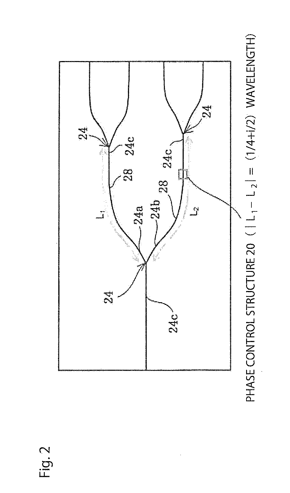
[0093]In this regard, the returning light of the two-stage branched optical waveguide 30 according to the present invention to which the phase control structure 20 including the optical waveguide of the light path length of λ / 4 is introduced as illustrated in FIG. 5 is considered. In the two-stage branched optical waveguide 30 to which the phase control structure 20 is introduced, the reflection light is generated in the one first stage optical branch section 24, and the two second stage optical branch sections 24, and the reflection light generated in the two second stage optical branch sections 24 returns to the input terminal 24c of the first stage optical branch section 24 through each of the first output terminal 24a and the second output terminal 24b of the first stage optical branch section 24.

[0094]Here, the optical waveguide of the light path length of λ / 4 is introduced to any one of the optical waveguides 28 connected to each of the first output term...

second embodiment

of Light Source Circuit

[0100]A multi-stage branched optical waveguide of three or more stages is able to be realized by simply performing the cascade connection with respect to the branched optical waveguide. In FIG. 6, the light source circuit including a four-stage branched optical waveguide 32 (a 16-branched optical waveguide) to which the phase control structure is introduced is illustrated. In the multi-stage branched optical waveguide 32 of three or more stages, according to the same principle as in the two-stage branched optical waveguide 30 described above, it is possible to completely inhibit the returning light caused by the optical branch section 24 after the second stage.

[0101]Thus, in the multi-stage branched optical waveguide 18 to which the phase control structure 20 is introduced, the reflection light from the optical branch section 24 after the second stage does not contribute to the returning light, and in the two-stage branched optical waveguide 30 or the multi-st...

third embodiment

of Light Source Circuit

[0110]The light propagated through the optical waveguide 28 has a property of being reflected in a portion where the structure is changed. For this reason, the reflection light may be generated in a connection portion between the optical waveguide 28 and the optical device 22. Thus, in order to inhibit the returning light caused by the optical device 22, the phase control structure 20 may be introduced between the optical device 22 and the previous-stage optical branch section 24 thereof as illustrated in FIG. 7.

[0111]For example, in this case, the phase control structure 20 may be an optical waveguide of a length for satisfying |L1−L2|=(¼+i / 2)λ (i=0, 1, 2, . . . ) when the light path lengths of the optical waveguide 28 between the input terminal of the optical device 22 and the two output terminals 24a and 24b of the previous-stage optical branch section 24 of the optical device are set to L1 and L2. Accordingly, it is possible to inhibit the returning light ...


PUM


Abstract

A light source circuit transmits light incident from a semiconductor laser source to a plurality of optical devices. At least one optical branch section is formed to branch one input-side optical waveguide at least into a first output-side optical waveguide terminal and a second output-side optical waveguide terminal. A light path length (L1) between the optical branch section and a next-stage optical branch section or the optical device is connected to the first output-side optical waveguide extending from the optical branch section and a light path length (L2) between the optical branch section and the next-stage optical branch section selected such that the absolute value of a difference between (L1) and (L2) is (¼+i / 2) times (i is zero or a positive integer) the wavelength of the light transmitted through the light source circuit.

Description

TECHNICAL FIELD[0001]The present invention relates to a light source circuit which is used in optical communication, an optical interconnection, and the like, and in particular, to a light source circuit in which a branched optical waveguide is formed on a substrate, and light incident from a light source is transmitted to a plurality of optical devices, and a light source device equipped with the light source circuit.BACKGROUND ART[0002]Recently, the study on silicon photonics in which various optical devices are integrated on a silicon substrate has received extensive attention.[0003]It is known that silicon is an indirect transition type material, and thus a light source with high energy efficiency is difficult to be realized using the silicon. On the other hand, a compound semiconductor such as GaAs (gallium arsenide) and InP (indium phosphide) is a direct transition type material, and thus a light source with high energy efficiency is able to be realized using the compound semi...

Claims


Application Information

Patent Timeline
IPC IPC(8): G02F1/225G02B6/42G02B6/125
CPCG02F1/225G02B6/125G02B2006/12142G02F2001/217G02B2006/12159G02B6/4296G02B6/2813G02F1/0147G02F1/3138G02F1/217
Inventor OKANO, MAKOTOMORI, MASAHIKOISHIZAKA, MASASHIGESHIMIZU, TAKANORIHATORI, NOBUAKI
Owner NEC CORP
Why Eureka
Try Eureka