Novel ITO crossover integrated capacitive touch screen and manufacturing method thereof

Inactive Publication Date: 2015-02-12
SHENZHEN BAOMING TECH
7 Cites 14 Cited by

AI-Extracted Technical Summary

Problems solved by technology

Just years ago, touch screens were not so popular in the market.
In capacitive touch screen with conventional design such defects as lower light transmittance and poor operating stability always exist.
Besides...

Benefits of technology

[0008]The first object of the present invention is to provide A novel ITO crossover integrated capacitive touch screen. Through improved design with its laminated structur...

Abstract

Disclosed are a novel ITO crossover integrated capacitive touch screen and a manufacturing method thereof. The novel ITO crossover integrated capacitive touch screen comprises a transparent substrate, and a silicon dioxide layer, a niobium pentoxide layer, a black resin layer, an ITO crossover electrode, a first insulation layer, an ITO electrode, a metal electrode, and a second insulation layer sequentially stacked on the transparent substrate. The silicon dioxide layer covers the glass completely, and the niobium pentoxide layer covers the silicon dioxide layer completely. The ITO electrode comprises a capacitive screen driver and a sensing electrode, and is provided with a patterned graphic structure. The capacitive screen driver and the sensing electrode are on the same layer, mutually independent, mutually insulated, and vertical in design. By the reasonable design for the stacked structure and the crossover conductive mode of the capacitive touch screen, the present invention can effectively improve the transmittance of the capacitive touch screen and reduce the visibility of the ITO pattern, and the reliability of the touch screen is further improved. novel ITO crossover integrated capacitive touch screen.

Application Domain

Technology Topic

Image

  • Novel ITO crossover integrated capacitive touch screen and manufacturing method thereof
  • Novel ITO crossover integrated capacitive touch screen and manufacturing method thereof
  • Novel ITO crossover integrated capacitive touch screen and manufacturing method thereof

Examples

  • Experimental program(1)

Example

[0031]In the following parts are further descriptions of the present invention with reference to the preferred embodiments.
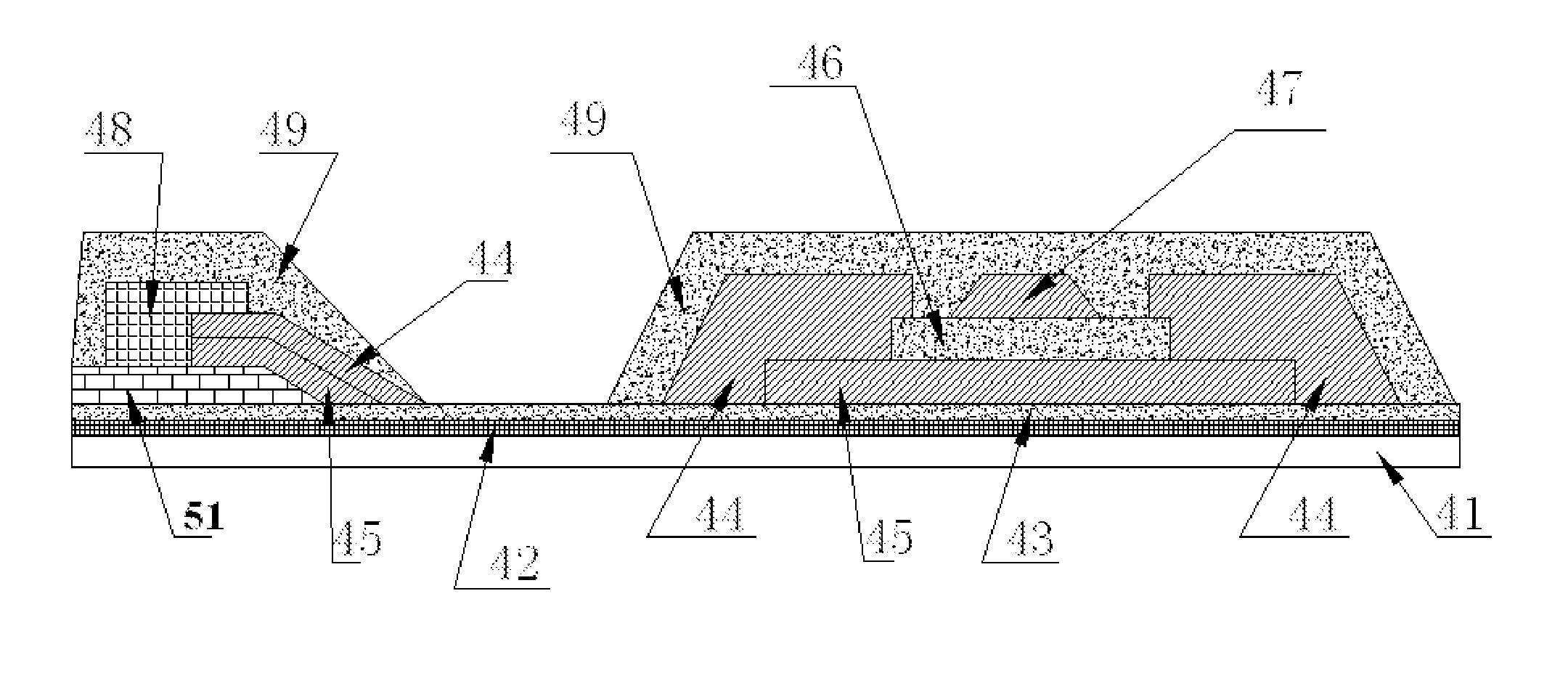
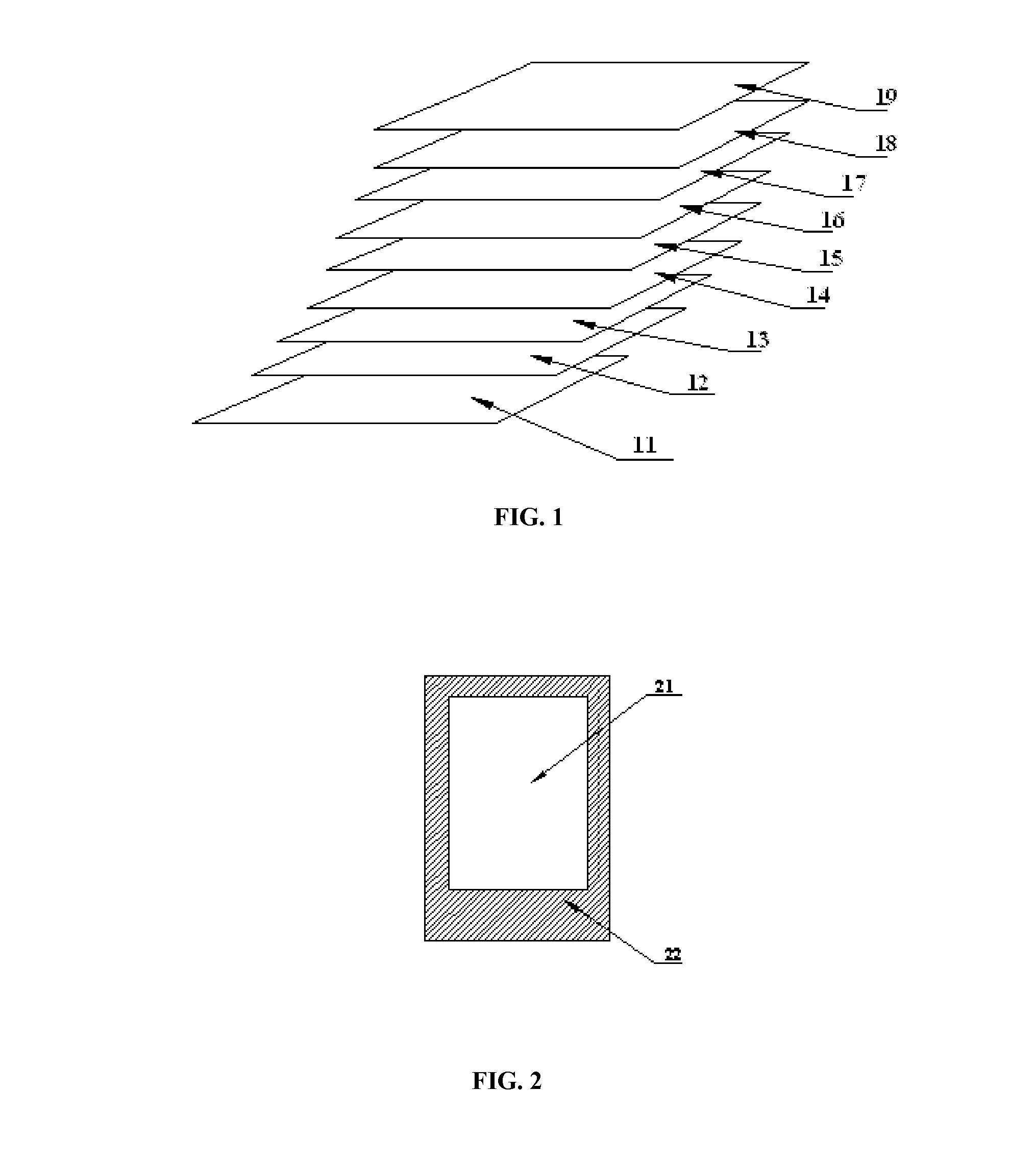
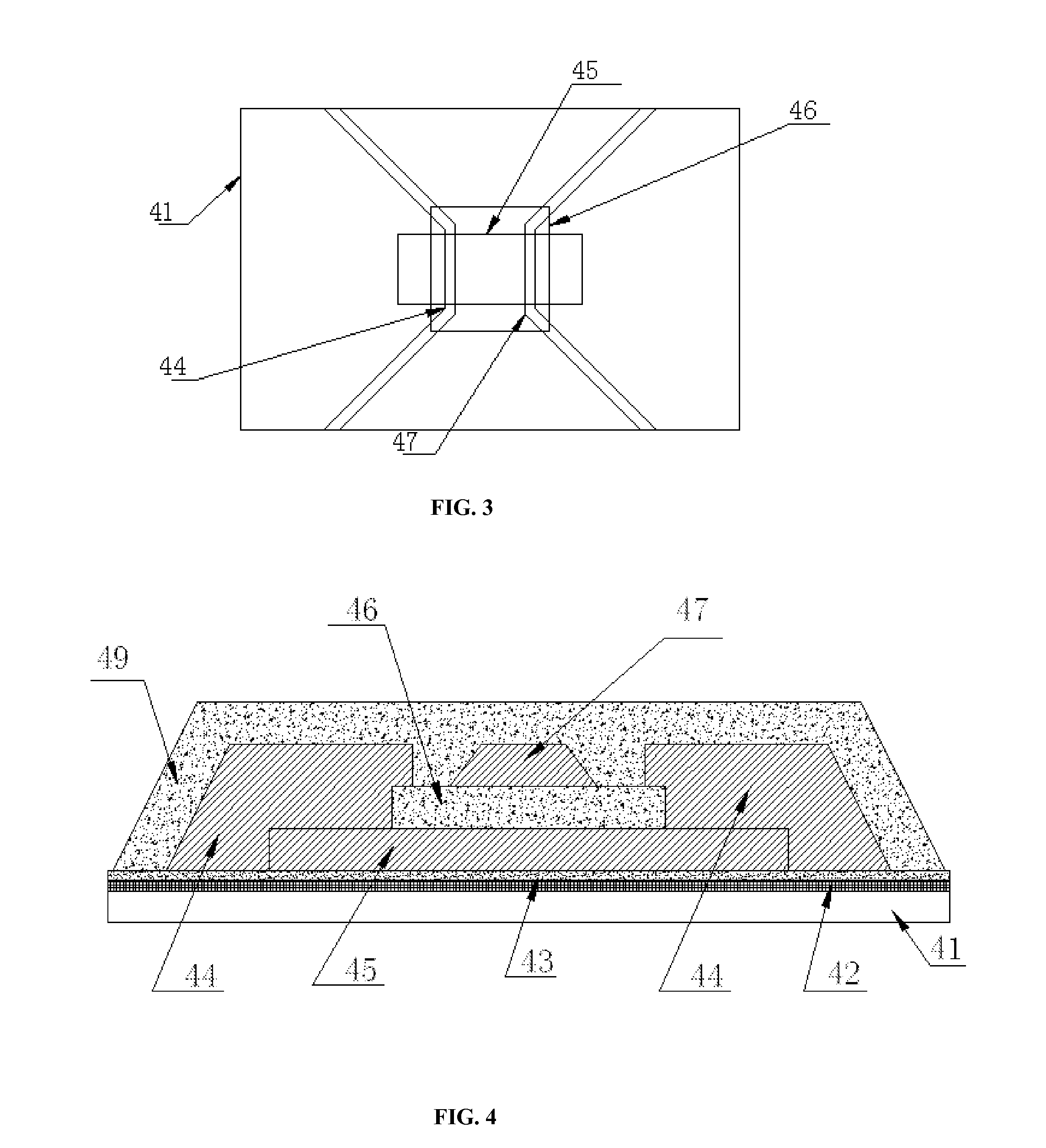
[0032]As shown in FIGS. 1 and 2, the said ITP crossover capacitive touch screen comprises of the chemically tempered glass substrate or resin substrate (thickness 0.5 mm˜2.0 mm) 11, and of the silica layer 12, niobium pentoxide layer 13, black resin layer 14, ITO crossover electrode 15, first insulation layer 16, ITO electrode 17, metal electrode 18 and second insulation layer 19 that are sequentially laminated on the transparent substrate. The said ITO crossover electrodes 15 include the crossover electrode in the display screen and overlapping electrode at the edge of the black-resin layer, both of which have regularly patterned structure, and can be shaped as rhombus, bar, square, snowflake or cross.
[0033]The said transparent substrate comprises of window section 21 and non-window section 22, with the black resin arranged in the non-window section 22 of the display screen.
[0034]The said black resin layer can shade not only the graphics layer of non-window section, but also the light and the visible things under the metal wire.
[0035]FIG. 3-6 are the enlarged diagram for local structure of and sectional view of the said ITO crossover capacitive touch screen of the preferred embodiment: ITO crossover electrode 45 includes crossover electrode 1 at the window section of the display screen and the crossover electrode 2 at the edge of the black resin layer 51, both of which have regularly patterned structure, and can be shaped as rhombus, bar, square, snowflake or cross. Crossover electrode 1 is connected to the drive wire 44 of ITO electrode 17 (right and left ends of ITO electrode 1) and induction wire 47(upper and lower ends of ITO electrode 2—not shown in the drawing). And crossover electrode 2 is connected to metal electrode 48 and the ITO electrode's drive wire 44 (ITO electrode 1) or induction wire 47 (ITO electrode 2) of ITO electrode, and prevents both of them from breaking at the slope of the black resin layer 51. The first insulation layer 46 insulates the ITO electrode's drive wire 44 (ITO electrode 1) and induction wire 47 (ITO electrode 2) to keep them from being conducted to each other. The bonding of the flexible PCB with ITO electrode signal conduction is realized through the metal electrode. The second insulation layer 49 protects the metal electrode 48 and ITO conductor and keeps them insulated from the air.
Manufacturing Process:
[0036]Formation of silica layer: Coat the transparent substrate with SiO2 to form a transparent SiO2 film with even thickness of 0, 50, 100, 300, 400, 700, 1000 or 1500 ANG;
Formation of niobium pentoxide layer: Coat the silica layer with Nb2O5 to form a transparent Nb2O5 film with even thickness of 0, 20, 50, 150, 200, 400, 500 or 1000 ANG;
First black resin is evenly spread to the transparent substrate 41(11) by spin-coating or blade-coating, with thickness of 0.3 μm˜5 μm. Then the resin is pre-baked, exposed and developed to create the needed black-resin section. The black-resin section is structured as trapezoid, with thickness of 0.3 μm˜5 μm in its middle and a bevel angle of 6-60 degrees at the edge. Such a gentle angle is designed in an attempt to prevent the ITO electrode from breaking in the case of the sharp thickness difference when ITO electrodes (drive wire ITO electrode 1 and induction wire ITO electrode 2) pass by the slope. The black resin area serves as the non-window section of the display screen to shade the metal electrode. The said black resin is made of protective light-sensitive photoresist (KE410 made by Taiwan Everlight Chemical). As a black negative photoresist, the material mainly consists of: acryl resin, epoxy resin, negative light-sensitive agent, propylene glyool monomethyl ether acetate (PMA) and black pigment, the actual ratio of which are as follows: 15˜30 (resin):60˜80 (PMA):1˜10 (black pigment and negative light-sensitive agent).
[0037]In forming the black resin layer, the pre-baking temperature is set as 60-150° C., time as 50-200 seconds and exposure energy as 100-500 mj. Na series or Ka series alkaline solution is used as developer, and developing temperature is set as 20-40° C. Then the black resin is hard baked under the temperature of 200-300° C. and for 0.5-3 hours. After the above processes, a black resin layer 51 (12) with regular pattern and thickness of 0.3 μm˜5 μm will be finally formed.
Formation of ITO crossover electrode: After the transparent glass substrate is chemically tempered, it will be ITO coated to make a transparent ITO film with even thickness of 50-2000 ANG (surface resistance 10-430 ohm); the said ITO electrode is made of In2O3 SnO2, whose mass ratio is 85˜95:5˜15. ITO coating can be performed through the means below: vacuum magnetic-enhanced sputtering, chemical vapor phase depositing, thermal evaporating and sol-gel method.
Coat a layer of positive photoresist on the ITO-coated transparent substrate, with even thickness of 1 μm˜5 μm; the said positive photoresist materials are mainly made up of propylene glyool monomethyl ether acetate, epoxy resin and positive light-sensitive material. The photoresist can be coated to the substrate by roll coating, spin coating, blade coating or other ways.
After the above processes, the photoresist will be pre-baked, exposed, developed, etched and released, and finally a 50-2000 ANG-thick layer of photoresist (surface resistance 10-430 ohm) and the regular ITO pattern or electrode will be formed. In forming the layer, the pre-baking temperature is set as 60-150° C., time as 50-200 seconds and exposure energy as 100-500 mj. Na series or Ka series alkaline solution is used as developer, and the developing temperature is set as 20-40° C. Hydrochloric acid and nitric acid are mixed by a certain proportion to make the ITO etching solution, with PH value as 1-3. The etching temperature is set as 40-50° C. Dimethylsulfoxide and cholamine are mixed under a proportion of 70%:30% to make the liquid to release the photoresist, with release temperature of 40-80° C.
Formation of first insulation layer:
Coat a layer of negative photoresist on the ITO-coated transparent substrate, with even thickness of 0.5 μm˜3 μm; the negative photoresist materials are mainly made up of propylene glyool monomethyl ether acetate, acryl resin, epoxy resin and negative light-sensitive agent. The photoresist can be coated to the substrate by roll coating, spin coating, blade coating or other ways.
After the above processes, the photoresist will be pre-baked, exposed and developed, and finally the regularly patterned insulation layer with thickness of 0.5˜3 μm will be formed. In forming layer, the pre-baking temperature is set as 60-150° C., time as 50-200 seconds and exposure energy as 100-500 mj. Na series or Ka series alkaline solution is used as developer, and developing temperature is set as 20-40° C. Then the insulation layer is hard baked under the temperature of 200-300° C. and for 0.5-3 hours. After the above processes, insulation layer 1 with regular pattern and thickness of 0.5 μm˜3 μm will be finally formed.
Formation of ITO electrode layer:
Coat a transparent ITO film on the transparent substrate with first insulation layer, with even thickness of 50-2000 ANG (surface resistance 10-430 ohm); the said ITO electrode is made of In2O3 SnO2, whose mass ratio is 85˜95:5˜15. ITO coating can be performed through the means below: vacuum magnetic-enhanced sputtering, chemical vapor phase depositing, thermal evaporating and sol-gel method.
Coat a layer of positive photoresist on the ITO-coated transparent substrate, with even thickness of 1 μm˜5 μm; the said positive photoresist materials are mainly made up of propylene glyool monomethyl ether acetate, epoxy resin and positive light-sensitive material. The photoresist can be coated to the substrate by roll coating, spin coating, blade coating or other ways.
After the above processes, the photoresist will be pre-baked, exposed, developed, etched and released, and finally a 50-2000 ANG-thick layer of photoresist (surface resistance 10-430 ohm) and the regular ITO pattern or electrode will be formed. In forming the layer, the pre-baking temperature is set as 60-150° C., time as 50-200 seconds and exposure energy as 100-500 mj. Na series or Ka series alkaline solution is used as developer, and the developing temperature is set as 20-40° C. Hydrochloric acid and nitric acid are mixed by a certain proportion to make the ITO etching solution, with PH value as 1-3. The etching temperature is set as 40-50° C. Dimethylsulfoxide and cholamine are mixed under a proportion of 70%:30% to make the liquid to release the photoresist, with release temperature of 40-80° C.
[0038]The said ITO electrode consists of capacitive screen driver (ITO electrode 1) and inductive electrode (ITO electrode 2), with regularly patterned structure. ITO electrode 1 and 2 are vertically designed on the same layer, but mutually independent and insulative.
Formation of metal electrode layer:
Coat a metal film on the transparent substrate with ITO electrode layer, with even thickness of 500-4000 ANG. The coated metal film is sandwich structured with stacked MoNb, AlNd and MoNb, whose thickness is respectively arranged as 50-500 ANG: 500-3000 ANG:50-500 ANG. In MoNb alloy, the mass ratio of Mo and Nb is 85˜95:5˜15, while in AlNd alloy, the mass ratio of Al and Nd is 95˜98:2˜5. The metal material can also be silver alloy or copper alloy compounded under a certain proportion. The process of vacuum magnetic-enhanced sputtering is employed here to make the metal film.
Coat a layer of positive photoresist on the metal-filmed transparent substrate, with even thickness of 1 μm˜5 μm; the said positive photoresist materials are mainly made up of propylene glyool monomethyl ether acetate, epoxy resin and positive light-sensitive material. The photoresist can be coated to the substrate by roll coating, spin coating, blade coating or other ways. After the above processes, the photoresist will be pre-baked, exposed, developed, etched and released, and finally a 500-4000 ANG-thick layer of photoresist (surface resistance 10-430 ohm) and the regular ITO pattern or electrode will be formed. In forming the layer, the pre-baking temperature is set as 60-150° C., time as 50-200 seconds and exposure energy as 100-500 mj. Na series or Ka series alkaline solution is used as developer, and the developing temperature is set as 20-40° C. Phosphoric acid, acetic acid and nitric acid are mixed by a certain proportion to make the metal etching solution. The etching temperature is set as 40-50° C. Dimethylsulfoxide and cholamine are mixed under a proportion of 70%:30% to make the liquid to release the photoresist, with release temperature of 40-80° C.
[0039]The wiring of the said metal electrode is only arranged in the black resin section, and no metal electrode is set in the window section.
Formation of second insulation layer:
Coat a layer of negative photoresist on the metal-coated transparent substrate, with even thickness of 0.5 μm˜3 μm; the negative photoresist materials are mainly made up of propylene glyool monomethyl ether acetate, acryl resin, epoxy resin and negative light-sensitive agent (POC A46 made by Taiwan Daxing Co.). The photoresist can be coated to the substrate by roll coating, spin coating, blade coating or other ways.
After the above processes, the photoresist will be pre-baked, exposed and developed, and finally the regularly patterned insulation layer with thickness of 0.5˜3 μm will be formed. In forming layer, the pre-baking temperature is set as 60-150° C., time as 50-200 seconds and exposure energy as 100-500 mj. Na series or Ka series alkaline solution is used as developer, and developing temperature is set as 20-40° C. Then the insulation layer is hard baked under the temperature of 200-300° C. and for 0.5-3 hours. After the above processes, insulation layer 1 with regular pattern and thickness of 0.5 μm˜3 μm will be finally formed.
[0040]With the upgrading of consumers' taste, in the case of electronic products, more emphasis is shifted to their quality. For single-body touch screen, consumers all the more stress its high transmittance, low reflectivity, invisibility of ITO pattern and high reliability. Thus higher requirements are proposed to us in designing the single-body touch screen.
[0041]In the present invention, due to the adoption of SiO2 and Nb2O5, which are properly arranged on the substrate to make an optimized thickness, the touch screen remarkably raises its transmittance and lowers the visuality of the pattern. Especially, when the thickness of SiO2 is set as 100-1000 ANG and Nb2O5 as 50-500 ANG, the transmittance of the product can be maintained as 93% or higher, and visuality controlled within Class 2, claiming a perfect effect. (Visuality classes are defined as follows: Class 0: completely unseen; Class 10: obviously seen. The higher the class is, the higher the visuality will be)
[0042]SiO2 features its anti-reflection and background-pattern reduction functions. For lights with different polarization states offer phases and amplitudes when reflected on film and air different from those when on film and lining interface, SiO2 can change the polarization state, lower product reflectivity and reduce visuality of pattern after film reflection. With the increase of the SiO2 film, some anti-reflection effect can be produced due to the film's interference. Ordinary glass can offer a reflectivity of about 5%, while glass coated with SiO2 can offer a reflectivity of about 2%. People's naked eyes can obviously see the ITO pattern on the glass with such pattern from a viewing angle, but can't obviously see the ITO pattern on SiO2-coated glass with such pattern.
[0043]If the films are laminated in the following order—black resin, SiO2 and Nb2O5, the manufacturing process can be adjusted as:
Formation of black-resin film: Coat the black resin on the transparent substrate through spin or blade process, with even thickness of 0.3 μm˜5 μm, and pre-bake, expose and develop the resin to form the black-resin section;
Formation of silica layer: Coat SiO2 on the black resin film to form a transparent silica layer, with even thickness of 100-1000 ANG;
Formation of Nb2O5 layer: Coat Nb2O5 on the silica layer to form a transparent Nb2O5 layer, with even thickness of 50-500 ANG;
Not many changes are needed for other processes.
[0044]The above descriptions constitute further information provided with reference with the detailed execution scheme of the present invention, but it shall not be considered that the execution of the present invention be limited to these contents. For regular technical personnel in the field of the invention, inductions or replacements are deemed to be within the protected scope of the present invention, so long as they don't break away from original conception.

PUM

no PUM

Description & Claims & Application Information

We can also present the details of the Description, Claims and Application information to help users get a comprehensive understanding of the technical details of the patent, such as background art, summary of invention, brief description of drawings, description of embodiments, and other original content. On the other hand, users can also determine the specific scope of protection of the technology through the list of claims; as well as understand the changes in the life cycle of the technology with the presentation of the patent timeline. Login to view more.

Similar technology patents

Classification and recommendation of technical efficacy words

  • Improve transmittance
  • Enhance reliability

Method and apparatus for automatic inspection of moving surfaces

InactiveUS6166393AEnhance reliabilityLess false alarm rateScattering properties measurementsInvestigating moving sheetsPhysicsFirst light
Owner:FRAUNHOFER GESELLSCHAFT ZUR FOERDERUNG DER ANGEWANDTEN FORSCHUNG EV +1
Why Eureka
Try Eureka