

Increasing ion/ioff ratio in finfets and nano-wires
a technology of ion/ioff ratio and nano-wires, which is applied in the direction of semiconductor devices, electrical apparatus, nanotechnology, etc., can solve the problems of insufficient cross-section, leakage through the middle of the fin, and the electric field generated by the gate control voltage when the device is in its off state can be limited in depth, so as to reduce the ion/ioff ratio, improve the chip yield, and improve the effect of circuits, components and systems
- Summary
- Abstract
- Description
- Claims
- Application Information
AI Technical Summary
Benefits of technology
Problems solved by technology
Method used
Image

Examples
Embodiment Construction
[0028]The following description is presented to enable any person skilled in the art to make and use the invention, and is provided in the context of a particular application and its requirements. Various modifications to the disclosed embodiments will be readily apparent to those skilled in the art, and the general principles defined herein may be applied to other embodiments and applications without departing from the spirit and scope of the present invention. Thus, the present invention is not intended to be limited to the embodiments shown, but is to be accorded the widest scope consistent with the principles and features disclosed herein.
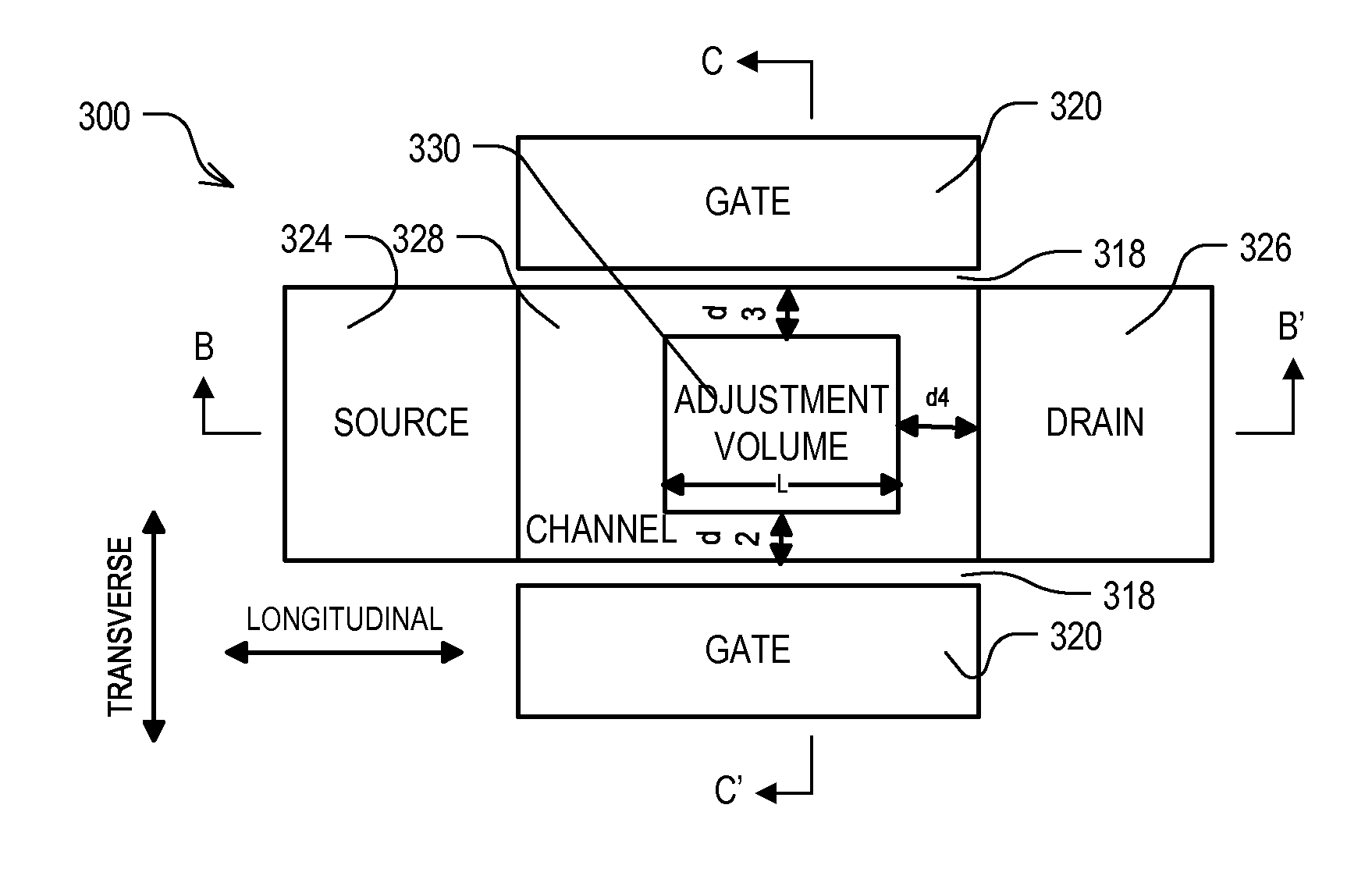
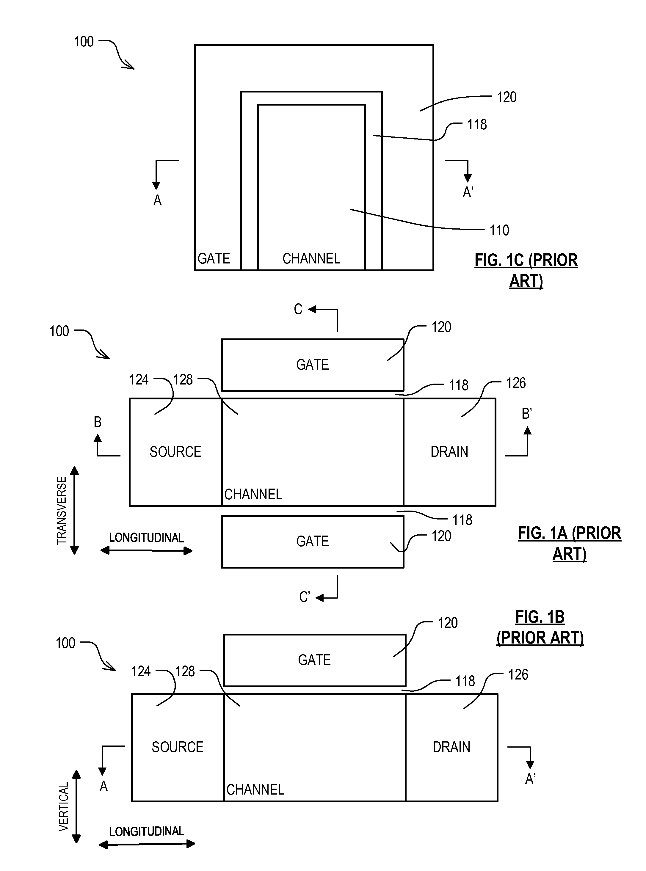
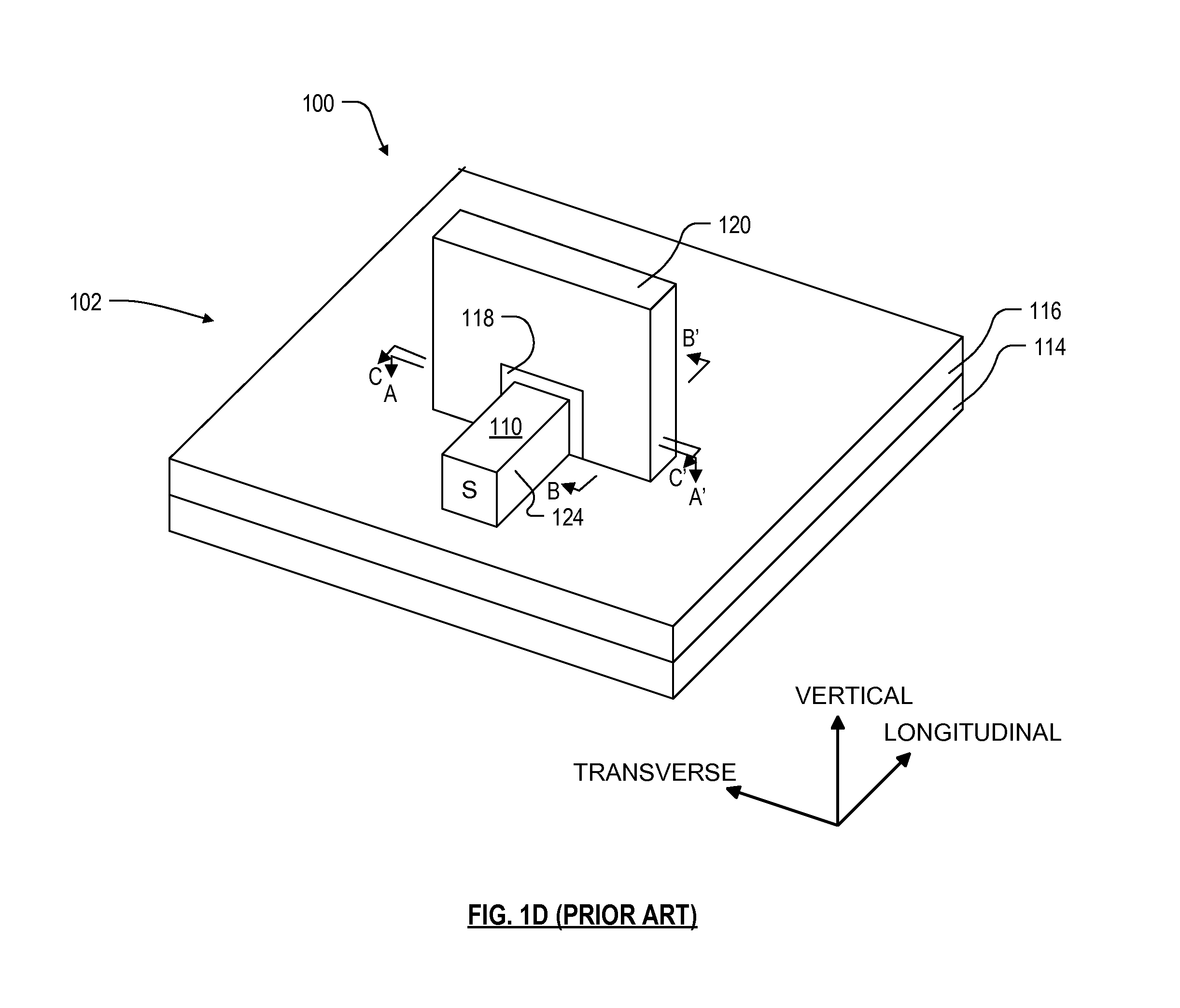
[0029]FIG. 1D is a perspective view of a simplified FinFET transistor 100 on an SOI wafer 102. As with all mechanical drawings herein, FIG. 1D is not drawn to scale. A bulk silicon substrate 114 underlies a buried oxide layer 116, and an undoped silicon layer above them has been patterned with a fin (body 110) having longitudinally separated so...
PUM
 Abstract
Description
Claims
Application Information