

Level shifter
a level shifter and level shifter technology, applied in logic circuits, pulse automatic control, pulse techniques, etc., can solve the problems of limited voltage conversion range and other problems, and achieve the effect of larger voltage conversion rang
- Summary
- Abstract
- Description
- Claims
- Application Information
AI Technical Summary
Benefits of technology
Problems solved by technology
Method used
Image

Examples
first embodiment
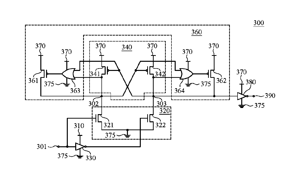
[0028]FIG. 3 is a circuit diagram of a level shifter 300 of the present invention. The level shifter 300 includes an input stage circuit 320, a latch circuit 340, and a transient speed-up circuit 360.
[0029]The input stage circuit 320 receives a first input signal and a second input signal. The voltage levels of the first input signal and the second input signal are in an input level section. The first input signal and the second input signal are out-of-phase. The input level section is determined by a voltage on an input reference voltage terminal 310.
[0030]The latch circuit 340 is coupled to the input stage circuit 320 through a first output terminal 302 and a second output terminal 303. The latch circuit 340 and the input stage circuit 320 determine the steady-state levels of the first output terminal 302 and the second output terminal 303 according to the first input signal and the second input signal. The latch circuit 340 forms a positive feedback changing the states of the fir...
second embodiment
[0042]FIG. 5 is a circuit diagram of a level shifter 500 of the present invention. The level shifter 500 includes an input stage circuit 520, a latch circuit 540, and a transient speed-up circuit 560. The circuit topologies and operation of the input stage circuit 520, the latch circuit 540, and the transient speed-up circuit 560 can be referred to the corresponding description of the input stage circuit 320, the latch circuit 340, and the transient speed-up circuit 360 of the level shifter 300 shown in FIG. 3. What is different from the transient speed-up circuit 360 is that, in transient speed-up circuit 560, the second input terminals of the first OR gate 563 and the second OR gate 564 are coupled to the first output terminal 502 and the second output terminal 503 through a first delay circuit 565 and a second delay circuit 566 respectively, wherein a logic delay time exists between a logic input signal and a logic output signal of each of the first delay circuit 565 and the seco...
third embodiment
[0047]FIG. 7 is a circuit diagram of a level shifter 700 of the present invention. The level shifter 700 includes an input stage circuit 720, a latch circuit 740, and a transient speed-up circuit 760. The circuit topologies and operation of the input stage circuit 720 and the latch circuit 740 can be referred to the corresponding description of the input stage circuit 320 and the latch circuit 340 of the level shifter 300 shown in FIG. 3. The transient speed-up circuit 760 includes a fifth transistor 761, a sixth transistor 762, a first NOR gate 763, and a second NOR gate 764. The first NOR gate 763 has a first input terminal, a second input terminal, and an output terminal. The first input terminal and the second input terminal of the first NOR gate 763 are coupled to the second output terminal 703 and the first output terminal 702 respectively, and the voltage level of an output signal of the first NOR gate 763 is in the output level section. A control terminal of the fifth transi...
PUM
 Abstract
Description
Claims
Application Information