Device for detecting quality level of microelectronic packaging samples using photo-thermal imaging

Inactive Publication Date: 2015-02-12
HUAZHONG UNIV OF SCI & TECH +1
View PDF2 Cites 14 Cited by
  • Summary
  • Abstract
  • Description
  • Claims
  • Application Information

AI Technical Summary

Benefits of technology

The patent is about a packaging process that uses multiple materials and the variations in heat conduction and light reflection to measure the depth of micropores and identify residue particles, cavities, and materials. The invention also improves the detection and evaluation of these features by integrating thermal imaging and light reflection intensity data. Additionally, the patent introduces the use of coaxial optical structures and zoom camera lens for more precise positioning and amplification of imaging. The invention also introduces the use of two motors for scanning and reducing the requirement for stiffness of the scanning structures.

Problems solved by technology

However, restricted by feature size, aspect ratio of a micropore, etc., various types of Through -Silicon-Via technologies still have many process problems to be solved.
Similar problems also exist in 2D flip-chip packaging, wafer level packaging and system level packaging based on embedded active components and passive components.

Method used


Image

  • Device for detecting quality level of microelectronic packaging samples using photo-thermal imaging
  • Device for detecting quality level of microelectronic packaging samples using photo-thermal imaging
  • Device for detecting quality level of microelectronic packaging samples using photo-thermal imaging

Examples


first embodiment

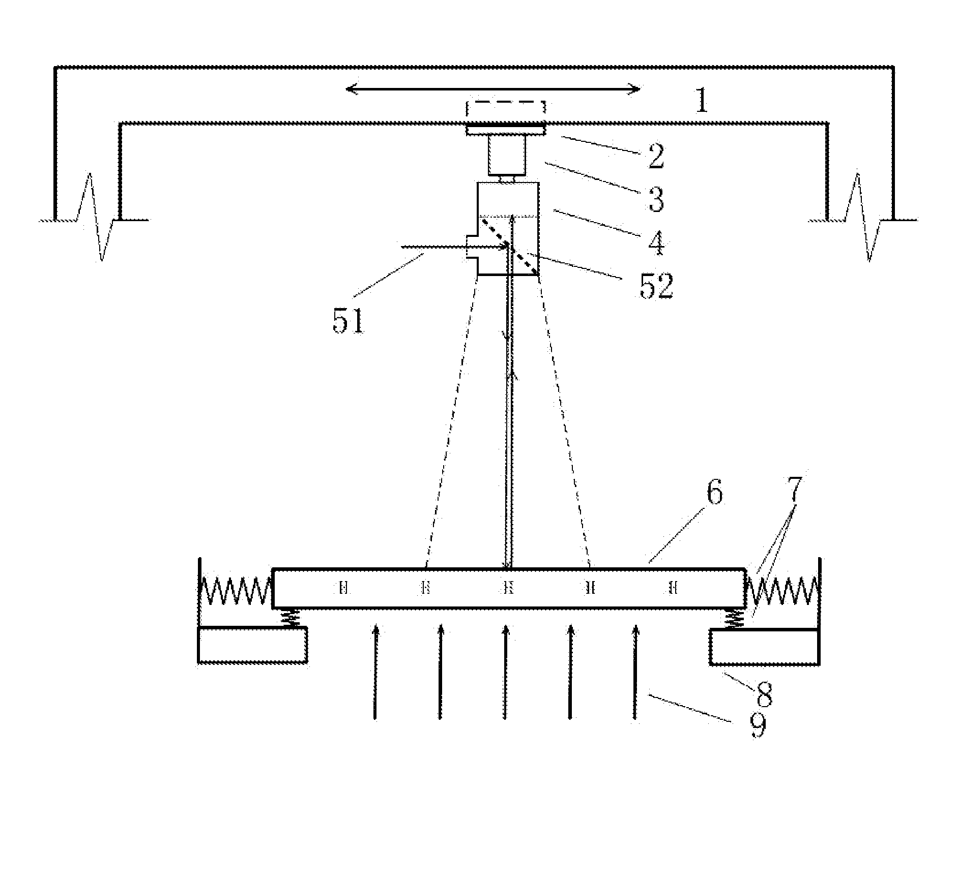
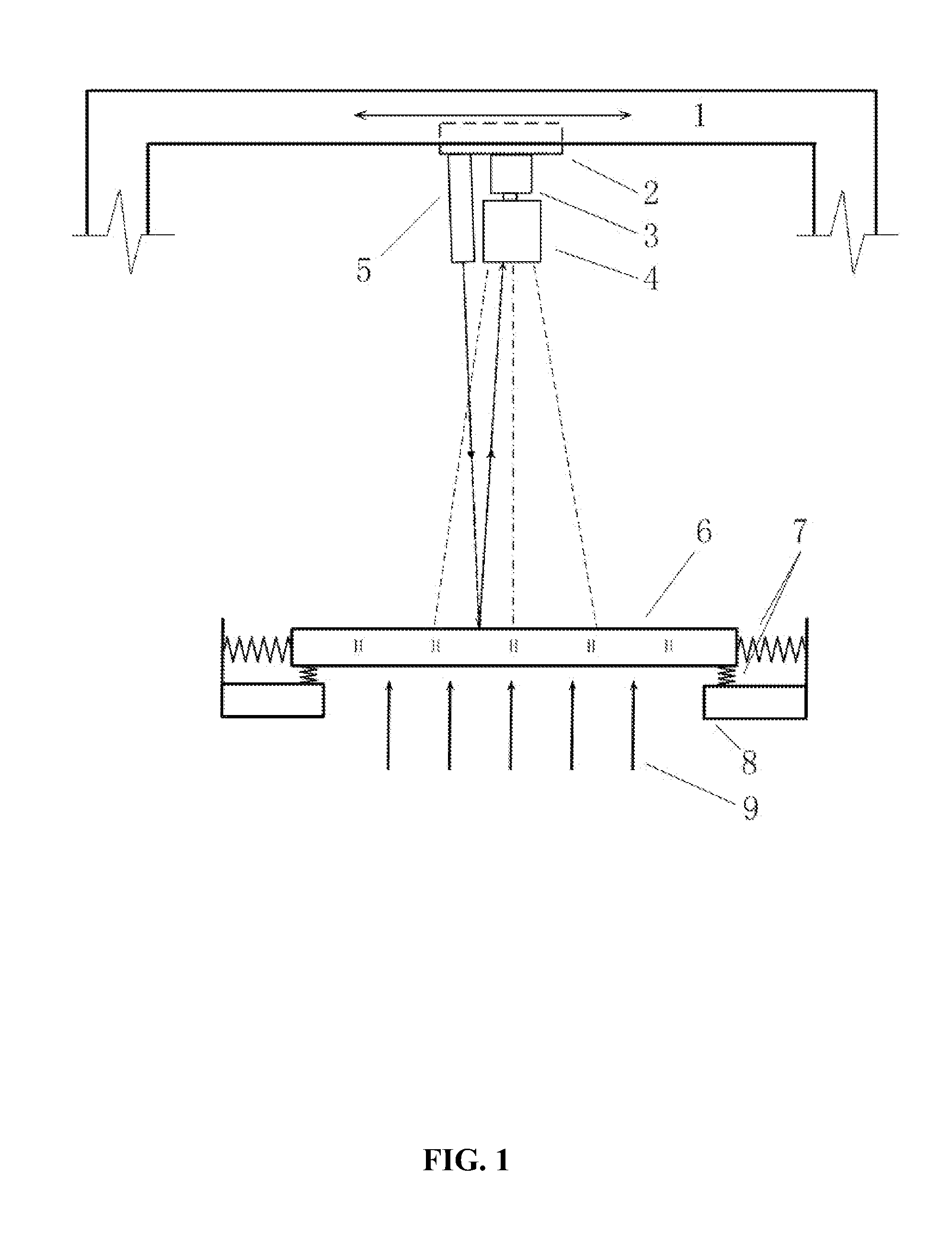
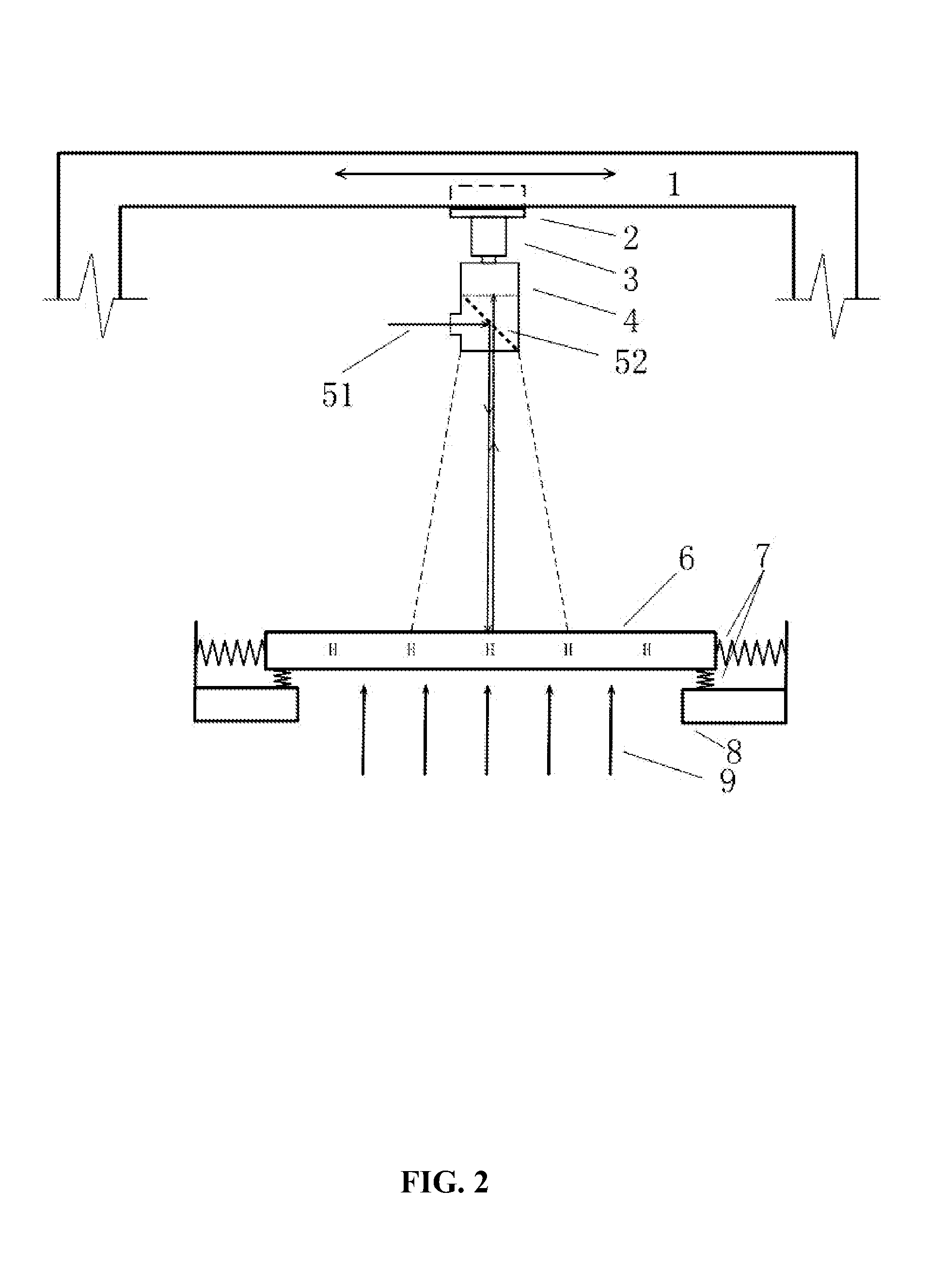
[0036]In the present invention, the support beam 1 is used for supporting, and the translational electric motor 2 is fixed to the lower surface of the beam by a bolt, the translational electric motor 2 contains a guide which is arranged in the same direction as the beam. The imaging probe and the light emitter 5 moves horizontally above the sample driven by the translational electric motor 2 so as to scan the surface of the sample for imaging, and scanning path and scanning positions of the translational electric motor 2 and each of the captured images of each of the scanning positions are controlled and recorded by the data processing device. The light emitter 5 moves driven by the translational electric motor 2 and light is emitted on the upper surface of the sample 6 by the light emitter 5. Light reflectivity varies due to differences in reflectivity of the material and differences in geometric depth of the irradiated position. Therefore, light intensity of the imaging signal of ...

second embodiment

[0042]In the present invention, both the incident light and the reflected light can be arranged perpendicular on the upper surface of the sample by connecting a coaxial optical device with a fiber. The coaxial optical device is an optical element coated with a transflective film, which can be connected to the front end of a camera or be integrated with a camera.

[0043]In the above two embodiments, the device for detecting quality of microelectronic packaging samples based on photo-thermal imaging further comprises an optical element located in the front of the light emitter and is configured to filter and calibrate light emitted from the light emitter so as to insure the uniformity of the incident light.

[0044]In the above two embodiments, the device for detecting quality of microelectronic packaging samples based on photo-thermal imaging further comprises a heating element disposed at the bottom of the sample and is configured to heat the lower surface of the sample 6 by radio freque...


PUM


Abstract

An image acquisition device based on photo-thermal imaging, including a support beam, a translational electric motor, an imaging probe, and a light emitter. The translational electric motor is fixed to the lower side of the beam, and the imaging probe is perpendicularly fixed to a moving block in the translational electric motor. The light emitter is connected to the moving block via an adjustable connection piece, and by adjusting the adjustable connection piece, light emitted by the light emitter enters the imaging probe after being reflected by a sample. The moving block in the translational electric motor is configured to move the light emitter and the imaging probe in the radial direction right above the sample. The light emitter is configured to emit light on the upper surface of the sample. The imaging probe is configured to image reflected light from the upper surface of the sample.

Description

CROSS-REFERENCE TO RELATED APPLICATIONS[0001]This application is a continuation-in-part of International Patent Application No. PCT / CN2012 / 084560 with an international filing date of Nov. 14, 2012, designating the United States, now pending, and further claims priority benefits to Chinese Patent Application No. 201210366219.4 filed Sep. 28, 2012. The contents of all of the aforementioned applications, including any intervening amendments thereto, are incorporated herein by reference. Inquiries from the public to applicants or assignees concerning this document or the related applications should be directed to: Matthias Scholl P. C., Attn.: Dr. Matthias Scholl Esq., 245 First Street, 18th Floor, Cambridge, Mass. 02142.BACKGROUND OF THE INVENTION[0002]1. Field of the Invention[0003]The invention relates to a device and method for detecting the quality level of microelectronic packaging samples using photo-thermal imaging.[0004]2. Description of the Related Art[0005]3D microelectronic ...

Claims


Application Information

Patent Timeline
IPC IPC(8): G01N21/95
CPCG01N21/9501G01N2201/102G01N2201/0638G01N2201/0636G01N21/95G01N25/72G01N21/55G01N2201/10
Inventor LIU, SHENGDAI, YIQUANGAN, ZHIYINWANG, XIAOPING
Owner HUAZHONG UNIV OF SCI & TECH
Why Eureka
Try Eureka