

Package structure having silicon through vias connected to ground potential
a technology of ground potential and package structure, which is applied in the direction of semiconductor devices, electrical apparatus, semiconductor/solid-state device details, etc., can solve problems such as device performance, and achieve the effect of improving the electrical performance of the package structure and keeping the cost of production in the acceptable level
- Summary
- Abstract
- Description
- Claims
- Application Information
AI Technical Summary
Benefits of technology
Problems solved by technology
Method used
Image

Examples
first embodiment
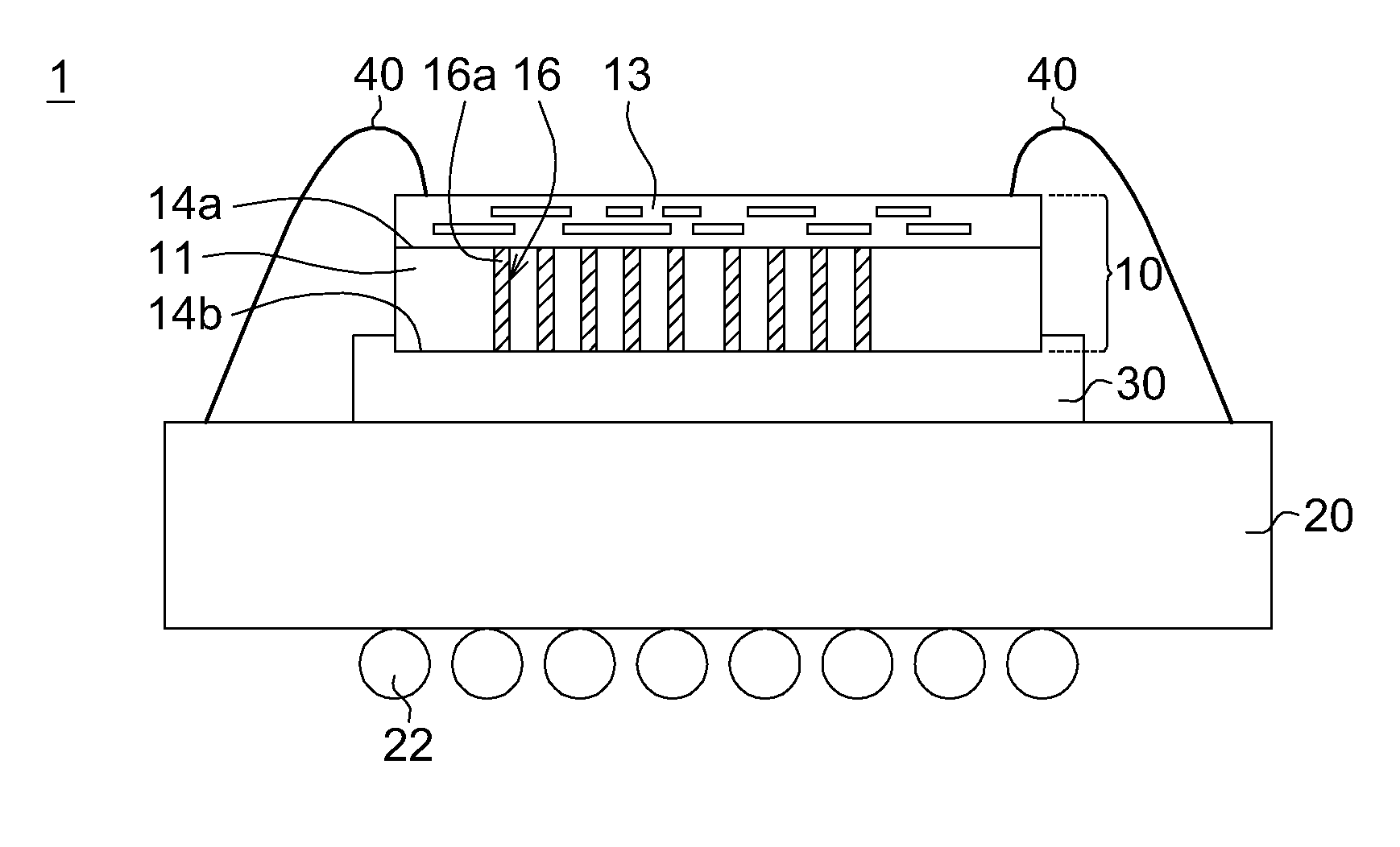
[0017]FIG. 1 schematically illustrates a package structure having TSVs connected to ground potential according to the first embodiment of the disclosure. A package structure 1 comprises a first device 10, a second device 20 and a conductive adhesive 30 disposed between the first device and the second device. The first device 10 comprises a substrate 11 having a front surface 14a (with an active layer 13 formed thereon) and a back surface 14b, and plural through silicon vias (TSVs) 16 filled with conductor 16a formed within the substrate 11 for connecting to grounding potential. Also, the package structure 1 further comprises plural wires 40, and the first device 10 is externally wire-bonded to the second device 20 by the wires. As shown in FIG. 1, the first device 10 is electrically connected to the second device 20 by wire bonding the front side of the first device 10 to the second device 20.
[0018]The conductive adhesive 30, such as a conductive die attach film (DAF), is disposed b...
second embodiment
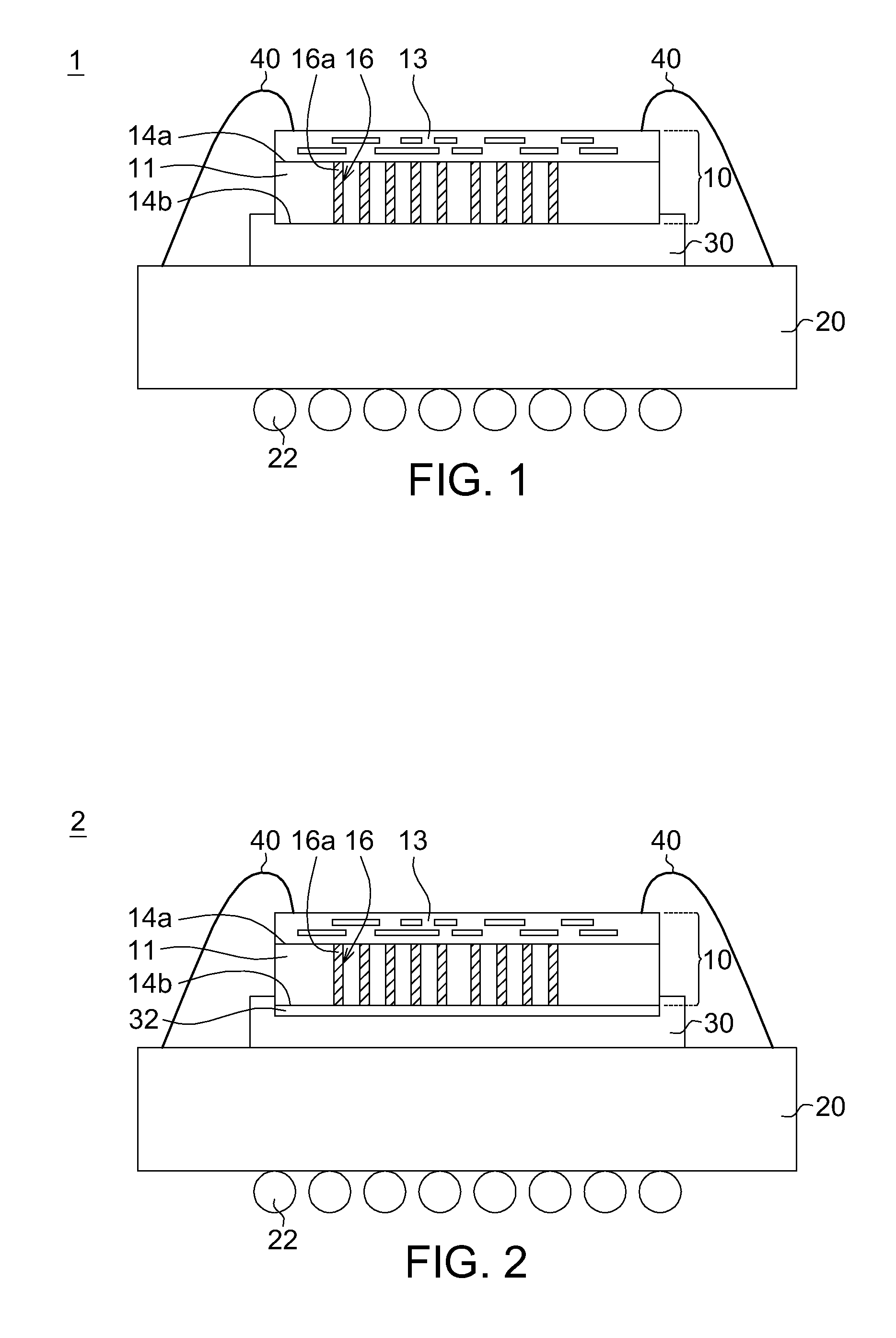
[0022]FIG. 2 schematically illustrates a package structure having TSVs connected to ground potential according to the second embodiment of the disclosure. The difference between the package structure of the second embodiment and the package structure of the first embodiment is addition of a conductive layer, such as a metal layer, between the first device 10 and the conductive adhesive 30.
[0023]As shown in FIG. 1, the conductive adhesive 30 of the first embodiment is formed on the back surface 14b of the first device 10, so as to electrically or physically contact the conductor 16a in the through silicon vias 16 (without the metal layer 32). According to the first embodiment, the electrical current passes the conductor 16a in the through silicon vias 16, the conductive adhesive 30, and reaches the grounding node (not depicted) of the second device 20.
[0024]Alternatively, the package structure 2 according to the second embodiment further comprises a metal layer 32 (such as a backside...
third embodiment
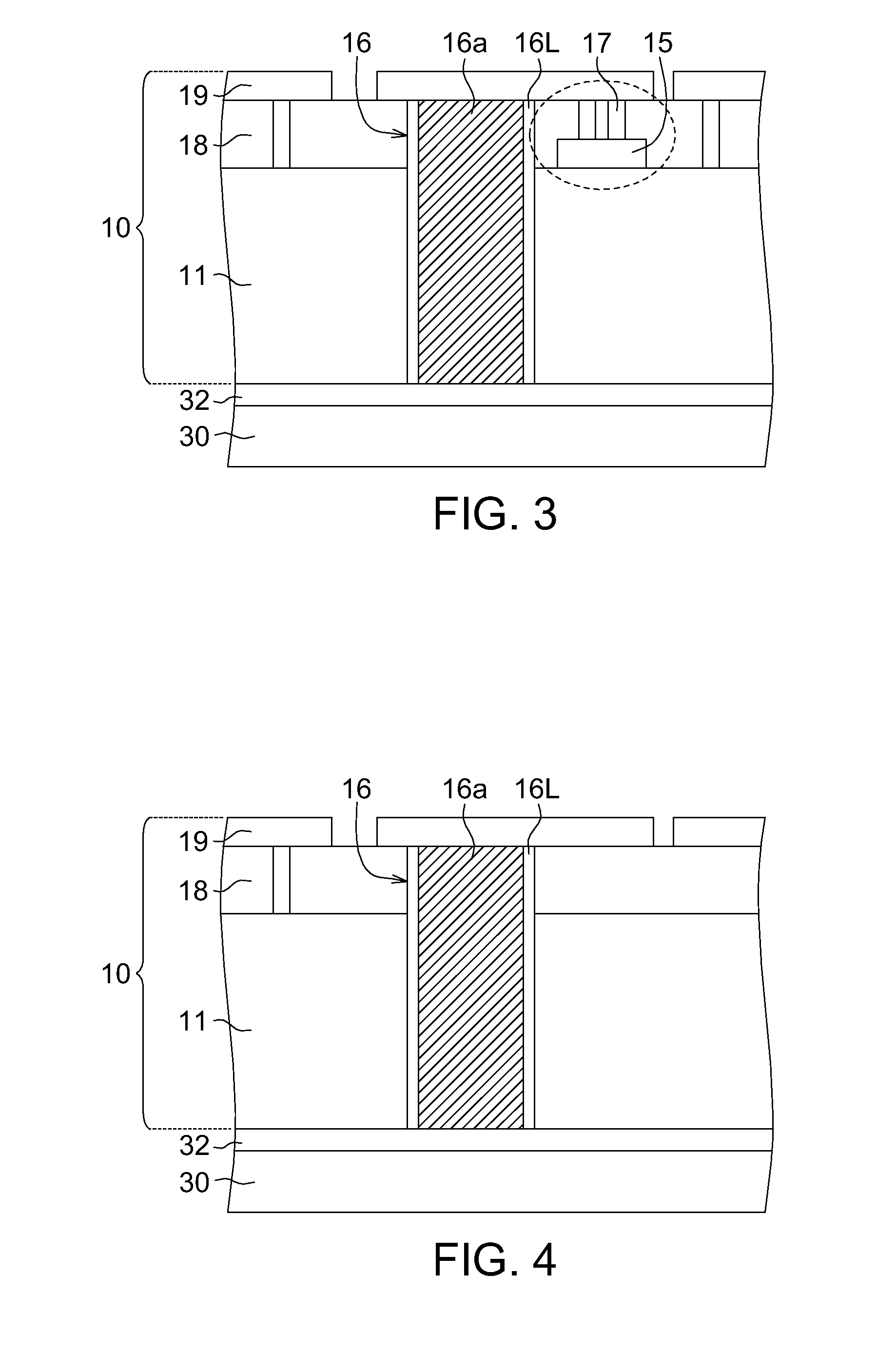
[0025]In the applications of present disclosure, the chips with different configurations could be applied in the package structure of the embodiment. For example, a chip with via-middle TSVs fabricated by a via-middle approach, or a chip with via-first TSVs fabricated by a via-first approach could be adopted as the first device of the package structure of the embodiment. The chips with different configurations in application are illustrated below. It is, of course, understood that these configurations are merely for demonstrating applicable structures, and not for limiting the disclosure.
[0026]FIG. 3 schematically illustrates a portion of a package structure having a chip with via-middle TSVs according to the third embodiment of the disclosure. In FIG. 3, a chip with via-middle TSVs (fabricated by a via-middle approach) is taken for exemplifying a first device in the package structure of the third embodiment. In the via-middle approach, the through silicon vias 16 filled with the co...
PUM
 Abstract
Description
Claims
Application Information