

Offset canceling dual stage sensing circuit
a sensing circuit and offset canceling technology, applied in the field of sensing circuitry, can solve problems such as reducing the switching speed of the mtj
- Summary
- Abstract
- Description
- Claims
- Application Information
AI Technical Summary
Benefits of technology
Problems solved by technology
Method used
Image

Examples
Embodiment Construction
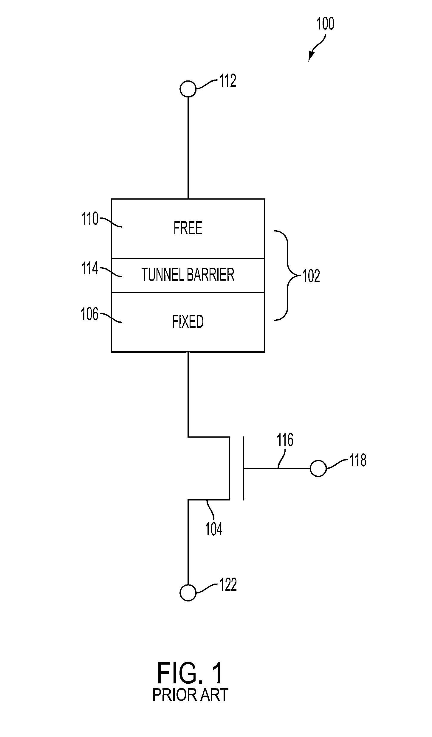
[0029]FIG. 1 illustrates a resistive memory element 100 including a magnetic tunnel junction (MTJ) 102 coupled to an access transistor 104. A free layer 110 of the MTJ 102 is coupled to a bit line 112. The access transistor 104 is coupled between a fixed layer 106 of the MTJ 102 and a fixed potential node 122. A tunnel barrier layer 114 is coupled between the fixed layer 106 and the free layer 110. The access transistor 104 includes a gate 116 coupled to a word line 118.
[0030]Synthetic anti-ferromagnetic materials may be used to form the fixed layer 106 and the free layer 110. For example, the fixed layer 106 may comprise multiple material layers including a CoFeB, and Ru layer and a CoFe layer. The free layer 110 may be an anti-ferromagnetic material such as CoFeB, and the tunnel barrier layer 114 may be MgO, for example.
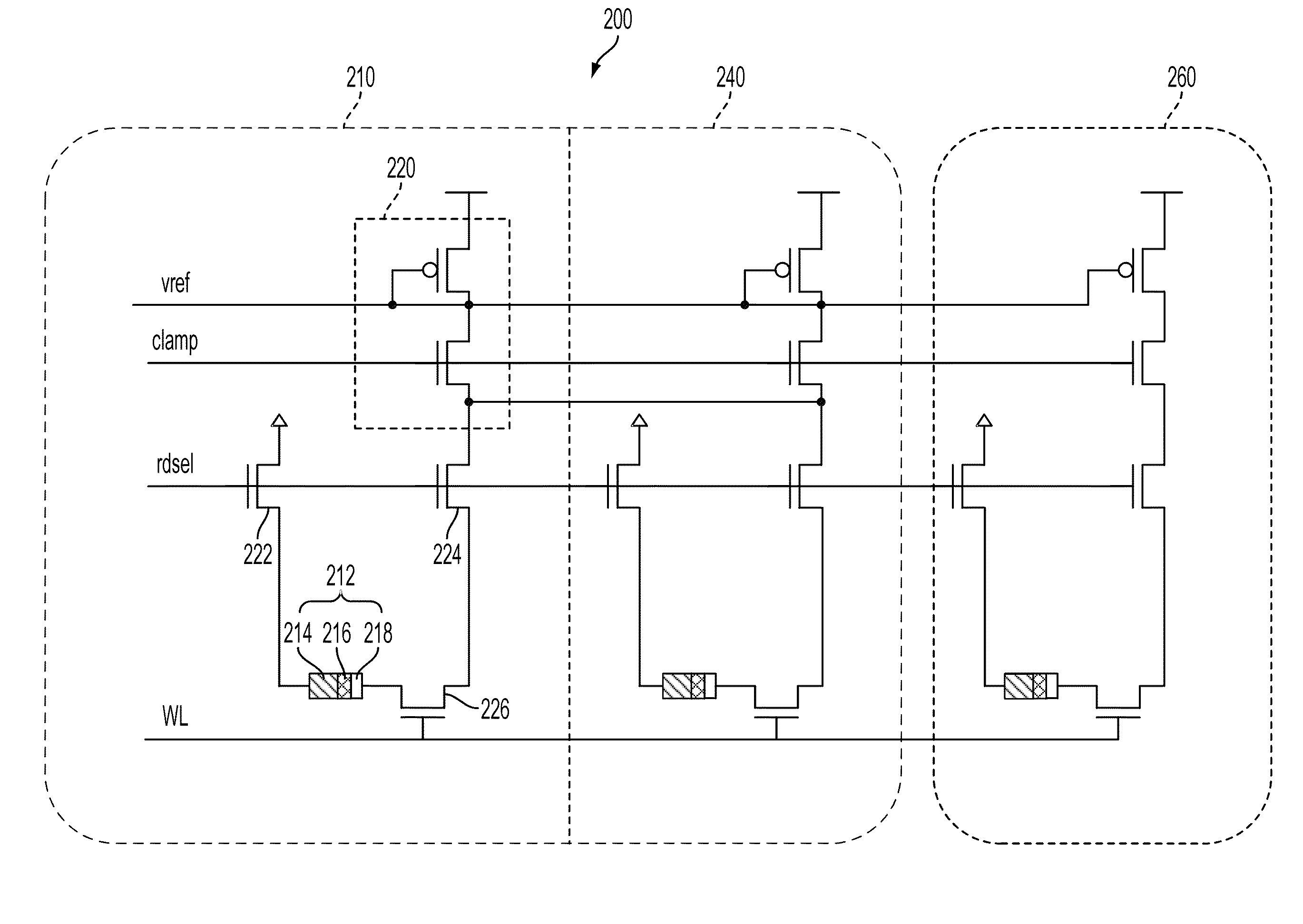
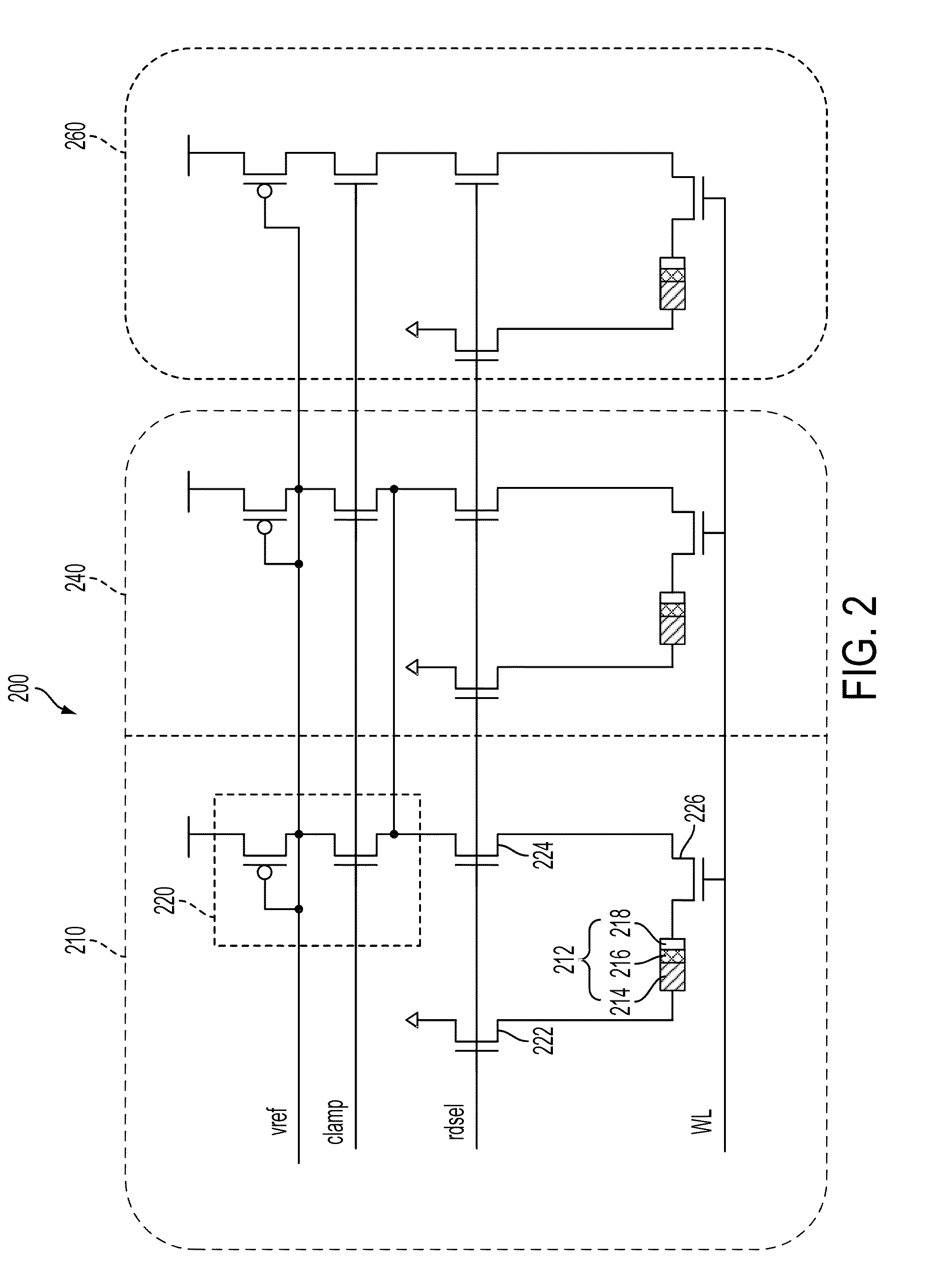
[0031]FIG. 2 is a circuit schematic illustrating a portion of a conventional magnetic random access memory (MRAM) 200. An MRAM 200 is divided into a data circuit 2...
PUM
 Abstract
Description
Claims
Application Information