Light emitting element manufacturing method, light emitting element and display panel

Active Publication Date: 2015-03-12
JOLED INC
View PDF0 Cites 2 Cited by
  • Summary
  • Abstract
  • Description
  • Claims
  • Application Information

AI Technical Summary

Benefits of technology

The present invention relates to a method of manufacturing a light-emitting element. The method allows for the creation of a structure where the energy rays are reflected upwards at the end sections of the inclined portion, resulting in a higher irradiation amount, while the central sections of the inclined portion have less irradiation because the energy rays are transmitted only once through the inclined portion. This results in a uniform film thickness of the functional layer as liquid repellency is greater at the central sections of the inclined portion. The method does not require any additional processes or increased complexity and is simple to implement.

Problems solved by technology

However, in recent years pixels are being made smaller, and therefore exposing only the end sections of the inclined portion to ultraviolet light is difficult and impractical, as mentioned above.
However, because forming the bank using two types of material that have different liquid repellency is complex, the manufacturing method of the light-emitting element also becomes complex.
On the other hand, by conventional manufacturing methods, in plan view, the central sections of the inclined portion overlap the upper surface of the reflective electrode, and therefore achieving uniform film thickness of the light-emitting layer is difficult.
Thus, it may be considered that film thickness at the central portion of the functional layer was thick because functional material was insufficient at the central portion of the opening.

Method used


Image

  • Light emitting element manufacturing method, light emitting element and display panel
  • Light emitting element manufacturing method, light emitting element and display panel
  • Light emitting element manufacturing method, light emitting element and display panel

Examples


embodiment 1

Schematic Structure of the Light-Emitting Element and Display Panel

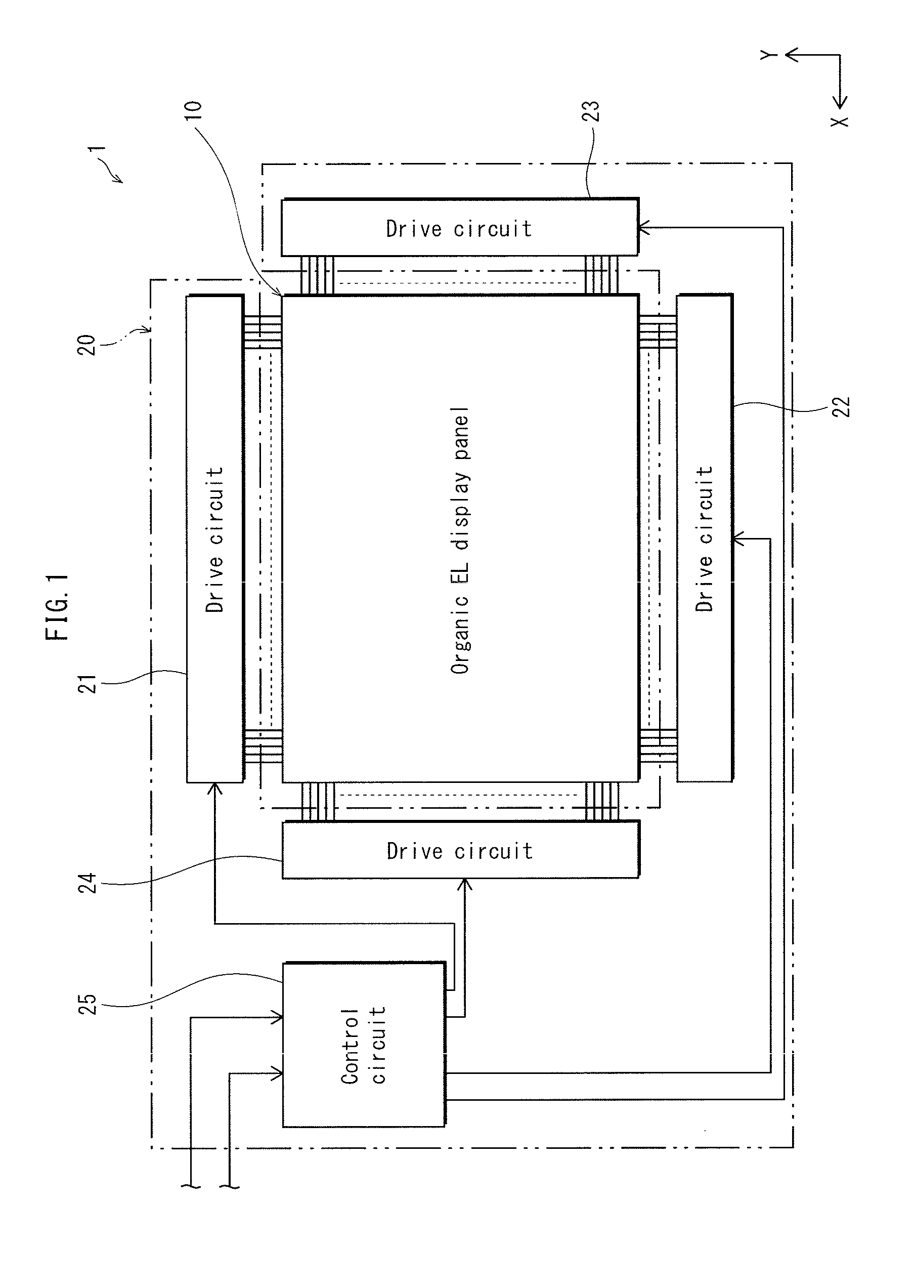
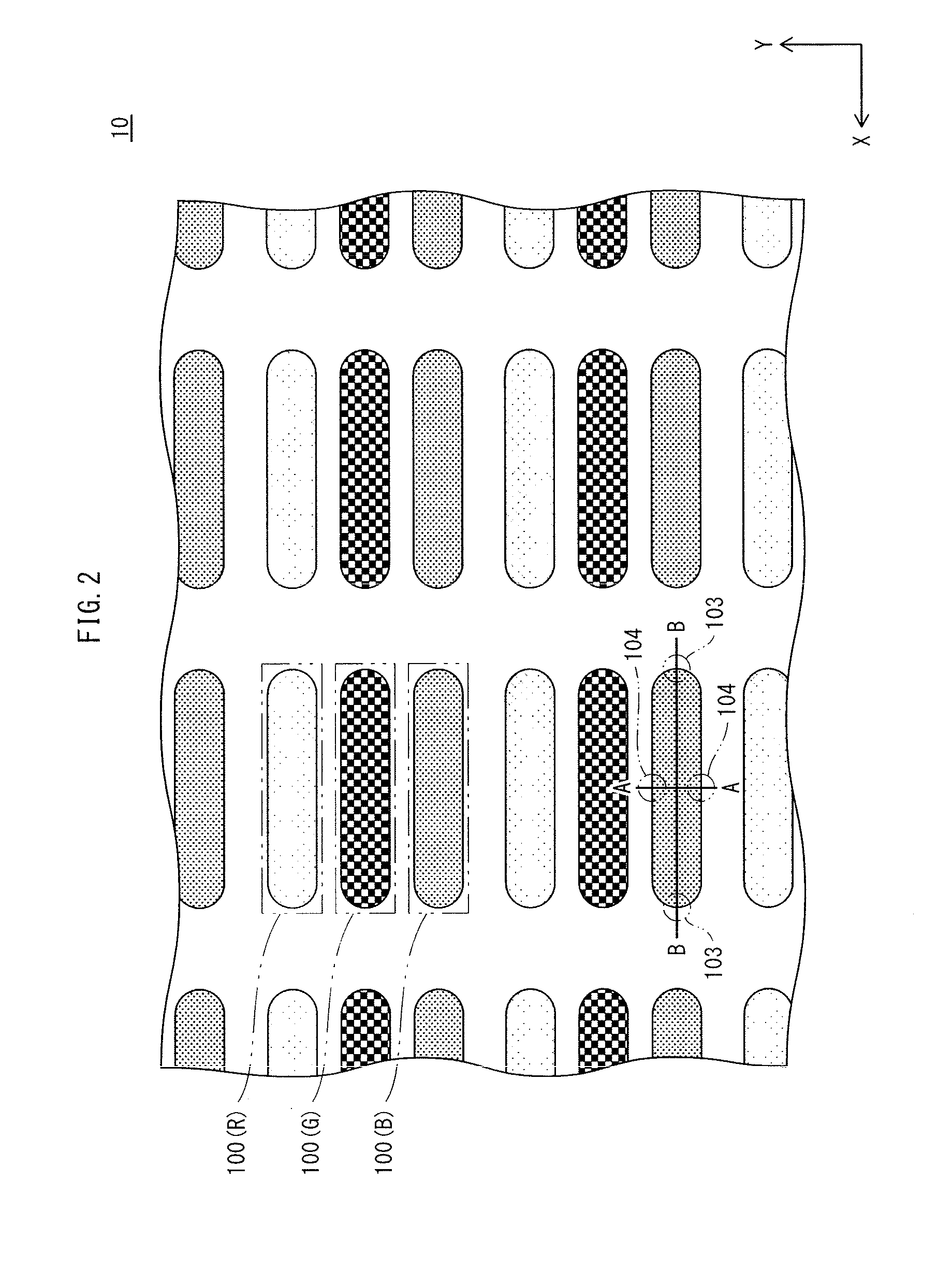
[0041]FIG. 1 is a diagram illustrating an overall structure of a display device including a display panel pertaining to embodiment 1. FIG. 2 is a plan view illustrating a portion of a surface of the display panel pertaining to embodiment 1.

[0042]A display device 1 illustrated in FIG. 1 is an organic EL display device used in a display, television, mobile telephone, etc., and includes a display panel 10, pertaining to embodiment 1, and a drive control section 20 connected to the display panel 10. The drive control section 20 includes four drive circuits 21-24 and a control circuit 25.

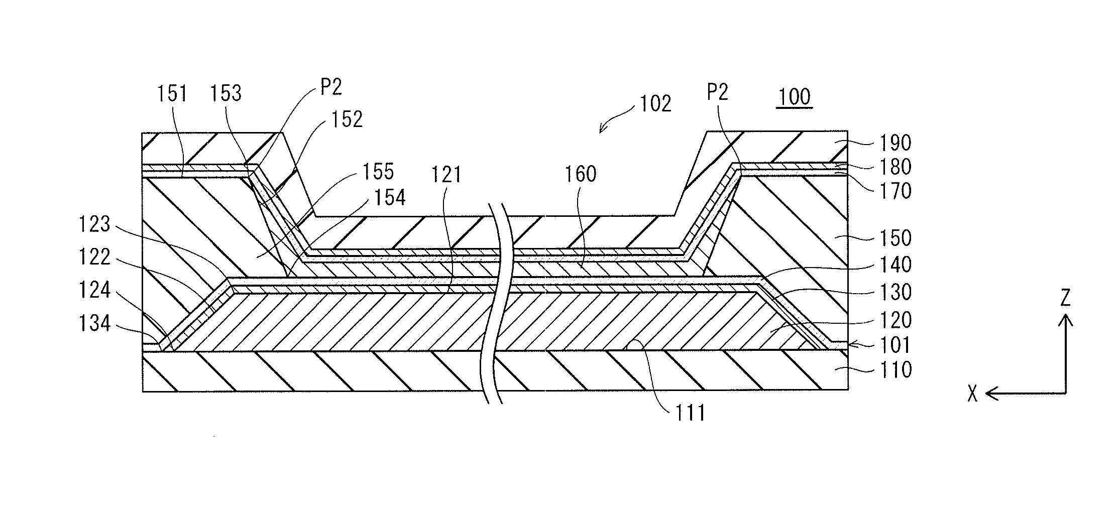
[0043]As illustrated in FIG. 2, the display panel 10 includes a plurality of light-emitting elements 100, each of which pertains to an aspect of the present invention. Each light-emitting element 100 is a sub-pixel that is red (R), green (G), or blue (B), and a pixel is composed of a set of one of each color (R, G, and B) of sub-pixel.

[00...

embodiment 2

[0103]A light-emitting element pertaining to embodiment 2 from the light-emitting element pertaining to embodiment 1 in that, in plan view, central sections of the inclined portion of the bank overlap neither the upper surface nor the side surface of the reflective electrode, whereas in the light-emitting element pertaining to embodiment 1 the central sections of the inclined portion do overlap with the side surface of the reflective electrode. Other points are essentially the same as in the light-emitting element pertaining to embodiment 1. The following is a description of only the points of difference between the light-emitting element pertaining to embodiment 2 and the light-emitting element pertaining to embodiment 1.

[0104]FIG. 11 is an end view illustrating a light-emitting element pertaining to embodiment 2, which is an end view of a cross-section taken along the A-A line in FIG. 2. FIGS. 12A and 12B are schematic views of a reflective electrode, light-transmissive electrode,...

embodiment 3

[0118]A light-emitting element pertaining to embodiment 3 differs from the light-emitting element pertaining to embodiment 1 in that the side surface of the reflective electrode is perpendicular to the upper surface of the substrate and that, in plan view, the reflective electrode has a substantially H shape, whereas in the light-emitting element pertaining to embodiment 1, the side surface of the reflective electrode is inclined and, in plan view, the reflective electrode has a rectangular shape. Other points are essentially the same as in the light-emitting element pertaining to embodiment 1. The following is a description of only the points of difference between the light-emitting element pertaining to embodiment 3 and the light-emitting element pertaining to embodiment 1.

[0119]FIGS. 14A-14C are schematic views of a reflective electrode, light-transmissive electrode, and bank of the light-emitting element pertaining to embodiment 3. FIG. 14A is a plan view, FIG. 14B is an end vie...


PUM


Abstract

A method of manufacturing a light-emitting element. The method includes forming an underlayer that includes a reflective electrode, forming a bank that has liquid repellency, irradiating the bank with characteristic energy rays to decrease liquid repellency of the bank, and forming a functional layer. The bank is formed on the underlayer and is provided with an opening and an inclined portion surrounding the opening. The opening has a shape that has a long axis and a short axis and is positioned above the reflective electrode. In plan view, end sections of the inclined portion in a direction of the long axis overlap the upper surface of the reflective electrode, while central sections of the inclined portion in the direction of the long axis do not overlap the upper surface of the reflective electrode.

Description

TECHNICAL FIELD[0001]The present invention relates to light-emitting element manufacturing methods, light-emitting elements, and display panels, and particularly to technology for forming functional layers of uniform film thickness by using coating methods.BACKGROUND ART[0002]Conventionally, in a light-emitting element manufacturing process, a functional layer such as a light-emitting layer, a hole transport layer, etc., is formed by application of ink containing functional material by a coating method such as an inkjet method. Inkjet methods include, for example, dropping ink into an opening provided in a bank, then forming a functional layer by drying the ink.[0003]Film thickness of the functional layer is preferably uniform, and in a case where film thickness is not uniform, uneven luminance can occur. However, when the opening in the bank into which ink is dropped has a shape that has a long axis and a short axis, an effect occurs such that film thickness of a central portion of...

Claims


Application Information

Patent Timeline
IPC IPC(8): H01L51/56H01L27/32H01L51/52
CPCH01L51/56H01L27/3246H01L51/5209H01L51/5218H05B33/10H05B33/26H10K59/122H10K71/191H10K50/818H10K71/00H10K50/813
Inventor TAKASHIGE, YUMEJI
Owner JOLED INC
Why Eureka
Try Eureka